MAX9315EUP+T Maxim Integrated Products, MAX9315EUP+T Datasheet - Page 4
MAX9315EUP+T
Manufacturer Part Number
MAX9315EUP+T
Description
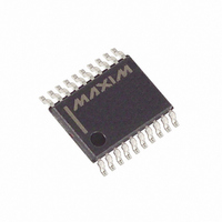
IC DRIVER DIFF 1:5 20-TSSOP
Manufacturer
Maxim Integrated Products
Type
Fanout Buffer (Distribution), Multiplexer , Datar
Datasheet
1.MAX9315EUP.pdf
(11 pages)
Specifications of MAX9315EUP+T
Number Of Circuits
1
Ratio - Input:output
2:5
Differential - Input:output
Yes/Yes
Input
HSTL, LVECL, LVPECL
Output
LVECL, LVPECL
Frequency - Max
1.5GHz
Voltage - Supply
2.25 V ~ 3.8 V
Operating Temperature
-40°C ~ 85°C
Mounting Type
Surface Mount
Package / Case
20-TSSOP
Frequency-max
1.5GHz
Lead Free Status / RoHS Status
Lead free / RoHS Compliant


AC ELECTRICAL CHARACTERISTICS
(V
to 80%), SEL = high or low, EN = low, V
V
1:5 Differential LVPECL/LVECL/HSTL
Clock and Data Driver
Note 1: Measurements are made with the device in thermal equilibrium.
Note 2: Current into a pin is defined as positive. Current out of a pin is defined as negative.
Note 3: DC parameters production tested at T
Note 4: Single-ended input operation using V
Note 5: Use V
Note 6: All pins open except V
Note 7: Guaranteed by design and characterization. Limits are set at ±6 sigma.
Note 8: Measured between outputs of the same part at the signal crossing points for a same-edge transition.
Note 9: Measured between outputs of different parts at the signal crossing points under identical conditions for a same-edge transition.
Note 10: Device jitter added to the input signal.
4
CC
PARAMETER
Differential Input-
to-Output Delay
Output-to-Output
Skew (Note 8)
Part-to-Part Skew
(Note 9)
Added Random
Jitter (Note 10)
Added
Deterministic Jitter
(Note 10)
Switching
Frequency
Output Rise/Fall
Time (20% to 80%)
CC
_______________________________________________________________________________________
- V
- V
EE
EE
, unless otherwise noted. Typical values are at V
= 2.375V to 3.8V, outputs loaded with 50Ω ±1% to V
BB
only for inputs that are on the same device as the V
SYMBOL
t
t
t
t
PLHD
SKOO
f
t
PHLD
SKPP
R
MAX
t
t
DJ
RJ
, t
F
,
CC
Figure 2
f
1.5Gbps 2E
PRBS pattern
(V
400mV,
Figure 2
Figure 2
and V
IN
OH
CONDITIONS
= 1.5GHz clock
IHD
- V
EE
= V
OL
.
) ≥
EE
BB
23
A
-1
= +25°C and guaranteed by design over the full operating temperature range.
+ 1.2V to V
is limited to V
CC
MIN
290
1.5
80
- V
CC
EE
CC
CC
, V
-40°C
TYP
ILD
0.8
= +3.3V, V
50
- V
- 2V, input frequency = 1.5GHz, input transition time = 125ps (20%
5
EE
= V
BB
= 3.0V to 3.8V.
MAX
reference.
EE
400
110
120
1.2
30
70
to V
IHD
CC
= V
MIN
310
1.5
90
- 0.15V, V
CC
+25°C
- 1V, V
TYP
0.8
20
50
IHD
ILD
MAX
440
130
130
1.2
40
70
- V
= V
ILD
CC
= 0.15V to the smaller of 3V or
MIN
300
- 1.5V.) (Notes 1, 7)
1.5
90
+85°C
TYP
0.8
20
50
MAX
520
220
145
1.2
50
70
ps (p-p)
p s
UNITS
GHz
ps
ps
ps
ps
ps
( RM S )
Related parts for MAX9315EUP+T
Image
Part Number
Description
Manufacturer
Datasheet
Request
R

Part Number:
Description:
Max9315 1 5 Differential Lvpecl/lvecl/hstl Clock And Data Driver
Manufacturer:
Maxim Integrated Products, Inc.
Datasheet:

Part Number:
Description:
MAX7528KCWPMaxim Integrated Products [CMOS Dual 8-Bit Buffered Multiplying DACs]
Manufacturer:
Maxim Integrated Products
Datasheet:
Part Number:
Description:
Single +5V, fully integrated, 1.25Gbps laser diode driver.
Manufacturer:
Maxim Integrated Products
Datasheet:
Part Number:
Description:
Single +5V, fully integrated, 155Mbps laser diode driver.
Manufacturer:
Maxim Integrated Products
Datasheet:
Part Number:
Description:
VRD11/VRD10, K8 Rev F 2/3/4-Phase PWM Controllers with Integrated Dual MOSFET Drivers
Manufacturer:
Maxim Integrated Products
Datasheet:
Part Number:
Description:
Highly Integrated Level 2 SMBus Battery Chargers
Manufacturer:
Maxim Integrated Products
Datasheet:
Part Number:
Description:
Current Monitor and Accumulator with Integrated Sense Resistor; ; Temperature Range: -40°C to +85°C
Manufacturer:
Maxim Integrated Products
Part Number:
Description:
TSSOP 14/A�/RS-485 Transceivers with Integrated 100O/120O Termination Resis
Manufacturer:
Maxim Integrated Products
Part Number:
Description:
TSSOP 14/A�/RS-485 Transceivers with Integrated 100O/120O Termination Resis
Manufacturer:
Maxim Integrated Products
Part Number:
Description:
QFN 16/A�/AC-DC and DC-DC Peak-Current-Mode Converters with Integrated Step
Manufacturer:
Maxim Integrated Products
Part Number:
Description:
TDFN/A/65V, 1A, 600KHZ, SYNCHRONOUS STEP-DOWN REGULATOR WITH INTEGRATED SWI
Manufacturer:
Maxim Integrated Products
Part Number:
Description:
Integrated Temperature Controller f
Manufacturer:
Maxim Integrated Products
Part Number:
Description:
SOT23-6/I�/45MHz to 650MHz, Integrated IF VCOs with Differential Output
Manufacturer:
Maxim Integrated Products
Part Number:
Description:
SOT23-6/I�/45MHz to 650MHz, Integrated IF VCOs with Differential Output
Manufacturer:
Maxim Integrated Products
Part Number:
Description:
EVALUATION KIT/2.4GHZ TO 2.5GHZ 802.11G/B RF TRANSCEIVER WITH INTEGRATED PA
Manufacturer:
Maxim Integrated Products