MAX9315EUP+T Maxim Integrated Products, MAX9315EUP+T Datasheet - Page 6
MAX9315EUP+T
Manufacturer Part Number
MAX9315EUP+T
Description
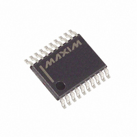
IC DRIVER DIFF 1:5 20-TSSOP
Manufacturer
Maxim Integrated Products
Type
Fanout Buffer (Distribution), Multiplexer , Datar
Datasheet
1.MAX9315EUP.pdf
(11 pages)
Specifications of MAX9315EUP+T
Number Of Circuits
1
Ratio - Input:output
2:5
Differential - Input:output
Yes/Yes
Input
HSTL, LVECL, LVPECL
Output
LVECL, LVPECL
Frequency - Max
1.5GHz
Voltage - Supply
2.25 V ~ 3.8 V
Operating Temperature
-40°C ~ 85°C
Mounting Type
Surface Mount
Package / Case
20-TSSOP
Frequency-max
1.5GHz
Lead Free Status / RoHS Status
Lead free / RoHS Compliant


The MAX9315 is a low-skew, 1-to-5 differential driver
designed for clock or data distribution. A 2-to-1 MUX
selects one of the two differential clock inputs, CLK0,
CLK0 or CLK1, CLK1. The MUX is switched by the sin-
gle-ended SEL input. A logic low selects the CLK0,
CLK0 input and a logic high selects the CLK1, CLK1
input. The SEL logic threshold is set by the internal volt-
age reference V
or by a single-ended LVPECL/LVECL signal. The
selected input is reproduced at five differential outputs.
The MAX9315 is synchronously enabled and disabled
with outputs in the low state to eliminate shortened
clock pulses. EN is connected to the input of an edge-
triggered D flip-flop. After power-up, drive EN low and
1:5 Differential LVPECL/LVECL/HSTL
Clock and Data Driver
6
18, 20
_______________________________________________________________________________________
PIN
10
11
12
13
14
15
16
17
19
1
2
3
4
5
6
7
8
9
BB
NAME
CLK0
CLK0
CLK1
CLK1
V
V
SEL
V
Q0
Q0
Q1
Q1
Q2
Q2
Q3
Q3
Q4
Q4
EN
CC
. SEL can be driven to V
BB
EE
Detailed Description
Noninverting Q0 Output. Typically terminate with 50Ω resistor to V
Inverting Q0 Output. Typically terminate with 50Ω resistor to V
Noninverting Q1 Output. Typically terminate with 50Ω resistor to V
Inverting Q1 Output. Typically terminate with 50Ω resistor to V
Noninverting Q2 Output. Typically terminate with 50Ω resistor to V
Inverting Q2 Output. Typically terminate with 50Ω resistor to V
Noninverting Q3 Output. Typically terminate with 50Ω resistor to V
Inverting Q3 Output. Typically terminate with 50Ω resistor to V
Noninverting Q4 Output. Typically terminate with 50Ω resistor to V
Inverting Q4 Output. Typically terminate with 50Ω resistor to V
Negative Supply Voltage
Clock Select Input (Single Ended). Drive low to select the CLK0, CLK0 input. Drive high to select the
CLK1, CLK1 input. The SEL threshold is equal to V
Noninverting Differential Clock Input 0. Internal 75kΩ pulldown to V
Inverting Differential Clock Input 0. Internal 75kΩ pullup to V
Reference Output Voltage. Connect to the inverting or noninverting clock input to provide a
reference for single-ended operation. When used, bypass with a 0.01µF ceramic capacitor to V
otherwise, leave open.
Noninverting Differential Clock Input 1. Internal 75kΩ pulldown to V
Inverting Differential Clock Input 1. Internal 75kΩ pullup to V
Positive Supply Voltage. Bypass V
capacitors as close to the device as possible with the smaller value capacitor closest to the device.
Output Enable Input. Outputs are synchronously enabled on the falling edge of the selected clock
input when EN is low. Outputs are synchronously driven low on the falling edge of the selected
clock input when EN is high.
Synchronous Enable
CC
and V
EE
CC
to V
toggle the selected clock input to enable the outputs.
The outputs are enabled on the falling edge of the
selected clock input after EN goes low. The outputs are
set to a low state on the falling edge of the selected
clock input after EN goes high. The threshold for EN is
equal to V
For interfacing to differential HSTL and LVPECL signals,
the V
grounded), allowing high-performance clock or data
distribution in systems with a nominal +2.5V or +3.3V
supply. For interfacing to differential LVECL, the V
range is -2.375V to -3.8V (with V
levels are referenced to V
LVPECL or LVECL, depending on the level of the V
supply. With V
EE
CC
with 0.1µF and 0.01µF ceramic capacitors. Place the
FUNCTION
range is from +2.375V to +3.8V (with V
BB
BB
.
.
CC
connected to a positive supply and
CC
CC
CC
CC
CC
CC
CC
and 75kΩ pulldown to V
and 75kΩ pulldown to V
- 2V.
- 2V.
- 2V.
- 2V.
- 2V.
CC
CC
CC
CC
CC
EE
EE
- 2V.
- 2V.
- 2V.
- 2V.
- 2V.
.
.
CC
Pin Description
CC
and are considered
grounded). Output
EE
EE
.
.
Supply
CC
;
CC
EE
EE
Related parts for MAX9315EUP+T
Image
Part Number
Description
Manufacturer
Datasheet
Request
R

Part Number:
Description:
Max9315 1 5 Differential Lvpecl/lvecl/hstl Clock And Data Driver
Manufacturer:
Maxim Integrated Products, Inc.
Datasheet:

Part Number:
Description:
MAX7528KCWPMaxim Integrated Products [CMOS Dual 8-Bit Buffered Multiplying DACs]
Manufacturer:
Maxim Integrated Products
Datasheet:
Part Number:
Description:
Single +5V, fully integrated, 1.25Gbps laser diode driver.
Manufacturer:
Maxim Integrated Products
Datasheet:
Part Number:
Description:
Single +5V, fully integrated, 155Mbps laser diode driver.
Manufacturer:
Maxim Integrated Products
Datasheet:
Part Number:
Description:
VRD11/VRD10, K8 Rev F 2/3/4-Phase PWM Controllers with Integrated Dual MOSFET Drivers
Manufacturer:
Maxim Integrated Products
Datasheet:
Part Number:
Description:
Highly Integrated Level 2 SMBus Battery Chargers
Manufacturer:
Maxim Integrated Products
Datasheet:
Part Number:
Description:
Current Monitor and Accumulator with Integrated Sense Resistor; ; Temperature Range: -40°C to +85°C
Manufacturer:
Maxim Integrated Products
Part Number:
Description:
TSSOP 14/A�/RS-485 Transceivers with Integrated 100O/120O Termination Resis
Manufacturer:
Maxim Integrated Products
Part Number:
Description:
TSSOP 14/A�/RS-485 Transceivers with Integrated 100O/120O Termination Resis
Manufacturer:
Maxim Integrated Products
Part Number:
Description:
QFN 16/A�/AC-DC and DC-DC Peak-Current-Mode Converters with Integrated Step
Manufacturer:
Maxim Integrated Products
Part Number:
Description:
TDFN/A/65V, 1A, 600KHZ, SYNCHRONOUS STEP-DOWN REGULATOR WITH INTEGRATED SWI
Manufacturer:
Maxim Integrated Products
Part Number:
Description:
Integrated Temperature Controller f
Manufacturer:
Maxim Integrated Products
Part Number:
Description:
SOT23-6/I�/45MHz to 650MHz, Integrated IF VCOs with Differential Output
Manufacturer:
Maxim Integrated Products
Part Number:
Description:
SOT23-6/I�/45MHz to 650MHz, Integrated IF VCOs with Differential Output
Manufacturer:
Maxim Integrated Products
Part Number:
Description:
EVALUATION KIT/2.4GHZ TO 2.5GHZ 802.11G/B RF TRANSCEIVER WITH INTEGRATED PA
Manufacturer:
Maxim Integrated Products