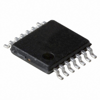
PCA2125TS/1,112 NXP Semiconductors, PCA2125TS/1,112 Datasheet - Page 21

PCA2125TS/1,112
Manufacturer Part Number
PCA2125TS/1,112
Description
IC CMOS RTC/CALENDAR 14-TSSOP
Manufacturer
NXP Semiconductors
Type
Clock/Calendar/Alarmr
Datasheet
1.PCA2125TS1112.pdf
(36 pages)
Specifications of PCA2125TS/1,112
Package / Case
14-TSSOP
Time Format
HH:MM:SS (12/24 hr)
Date Format
YY-MM-DD-dd
Interface
SPI, 3-Wire Serial
Voltage - Supply
1.3 V ~ 5.5 V
Operating Temperature
-40°C ~ 125°C
Mounting Type
Surface Mount
Function
Clock, Calendar
Supply Voltage (max)
5.5 V
Supply Voltage (min)
1.3 V
Maximum Operating Temperature
+ 125 C
Minimum Operating Temperature
- 40 C
Mounting Style
SMD/SMT
Rtc Bus Interface
Serial
Lead Free Status / RoHS Status
Lead free / RoHS Compliant
For Use With
OM6292 - DEMO BOARD PCA2125 RTC
Memory Size
-
Lead Free Status / RoHS Status
Lead free / RoHS Compliant, Lead free / RoHS Compliant
Other names
935283386112
PCA2125TS/1
PCA2125TS/1
PCA2125TS/1
PCA2125TS/1
NXP Semiconductors
PCA2125_1
Product data sheet
8.8 Clock output
8.9 External clock test mode
A programmable square wave is available at pin CLKOUT. Operation is controlled by
control bits COF[2:0] in register CLKOUT_control (0Dh). Frequencies of 32.768 kHz
(default) down to 1 Hz can be generated for use as a system clock, microcontroller clock,
input to a charge pump, or for calibration of the oscillator.
Pin CLKOUT is an open-drain output and enabled at power-on. When disabled the output
is LOW.
The duty cycle of the selected clock is not controlled, but due to the nature of the clock
generation, all clock frequencies, except 32.768 kHz, have a duty cycle of 50 : 50.
The ‘stop’ function can also affect the CLKOUT signal, depending on the selected
frequency. When ‘stop’ is active, the CLKOUT pin will generate a continuous LOW for
those frequencies that can be stopped. For more details, see
Table 35.
[1]
A test mode is available which allows for on-board testing. In this mode it is possible to set
up test conditions and control the operation of the RTC.
The test mode is entered by setting bit EXT_TEST in register Control_1 making
pin CLKOUT an input. The test mode replaces the internal signal with the signal applied to
pin CLKOUT. Every 64 positive edges applied to pin CLKOUT generates an increment of
one second.
The signal applied to pin CLKOUT should have a minimum HIGH width of 300 ns and a
minimum period of 1000 ns. The internal clock, now sourced from pin CLKOUT, is divided
down to 1 Hz by a 2
be set into a known state by using bit STOP. When bit STOP is set, the prescaler is reset
to 0. STOP must be cleared before the prescaler can operate again.
From a stop condition, the first 1 second increment will take place after 32 positive edges
on pin CLKOUT. Thereafter, every 64 positive edges will cause a 1 second increment.
Remark: Entry into test mode is not synchronized to the internal 64 Hz clock. When
entering the test mode, no assumption as to the state of the prescaler can be made.
Operation example:
Bits COF[2:0]
000
001
010
011
100
101
110
111
Duty cycle definition: HIGH-level time (%) : LOW-level time (%).
CLKOUT frequency selection
CLKOUT frequency (Hz)
32768
16384
8192
4096
2048
1024
1
CLKOUT = LOW
6
divide chain called a prescaler; see
Rev. 01 — 28 July 2008
Typical duty cycle
60 : 40 to 40 : 60
50 : 50
50 : 50
50 : 50
50 : 50
50 : 50
50 : 50
Section
SPI Real-time clock/calendar
Section
[1]
(%)
8.10. The prescaler can
8.10.
PCA2125
© NXP B.V. 2008. All rights reserved.
Effect of ‘stop’
no effect
no effect
no effect
CLKOUT = LOW
CLKOUT = LOW
CLKOUT = LOW
CLKOUT = LOW
21 of 36


