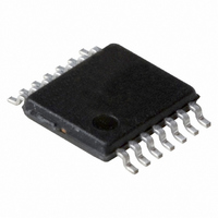
PCA2125TS/1,112 NXP Semiconductors, PCA2125TS/1,112 Datasheet - Page 24

PCA2125TS/1,112
Manufacturer Part Number
PCA2125TS/1,112
Description
IC CMOS RTC/CALENDAR 14-TSSOP
Manufacturer
NXP Semiconductors
Type
Clock/Calendar/Alarmr
Datasheet
1.PCA2125TS1112.pdf
(36 pages)
Specifications of PCA2125TS/1,112
Package / Case
14-TSSOP
Time Format
HH:MM:SS (12/24 hr)
Date Format
YY-MM-DD-dd
Interface
SPI, 3-Wire Serial
Voltage - Supply
1.3 V ~ 5.5 V
Operating Temperature
-40°C ~ 125°C
Mounting Type
Surface Mount
Function
Clock, Calendar
Supply Voltage (max)
5.5 V
Supply Voltage (min)
1.3 V
Maximum Operating Temperature
+ 125 C
Minimum Operating Temperature
- 40 C
Mounting Style
SMD/SMT
Rtc Bus Interface
Serial
Lead Free Status / RoHS Status
Lead free / RoHS Compliant
For Use With
OM6292 - DEMO BOARD PCA2125 RTC
Memory Size
-
Lead Free Status / RoHS Status
Lead free / RoHS Compliant, Lead free / RoHS Compliant
Other names
935283386112
PCA2125TS/1
PCA2125TS/1
PCA2125TS/1
PCA2125TS/1
NXP Semiconductors
PCA2125_1
Product data sheet
8.11 3-line SPI
Data transfer to and from the device is made via a 3-wire SPI-bus; see
lines for input and output are split. The data input and output lines can be connected
together to facilitate a bidirectional data bus. The chip enable signal is used to identify the
transmitted data. Each data transfer is a byte, with the Most Significant Bit (MSB) sent
first; see
Table 37.
The transmission is controlled by the active HIGH chip enable signal CE. The first byte
transmitted is the command byte. Subsequent bytes will be either data to be written or
data to be read. Data is captured on the rising edge of the clock and transferred internally
on the falling edge.
The command byte defines the address of the first register to be accessed and the
read/write mode. The address counter will auto increment after every access and will
reset to zero after the last valid register is accessed. The read/write bit (R/W) defines if the
following bytes will be read or write information.
Table 38.
In
10 minutes.
Pin
CE
SCL
SDI
SDO
Bit
7
6 to 4
3 to 0
Fig 18. Data transfer overview
Figure 19
Function
chip enable input
serial clock input
serial data input
serial data output
Figure
Symbol
R/W
SA
RA
Serial interface
Command byte definition
chip enable
the Seconds register is set to 45 seconds and the Minutes register to
data bus
18.
Value
0
1
001
00h to 0Fh register address range
Rev. 01 — 28 July 2008
COMMAND
Description
when LOW, the interface is reset; pull-down resistor included; active
input can be higher than V
permanently
when pin CE = LOW, this input might float; input can be higher than
V
when pin CE = LOW, this input might float; input can be higher than
V
push-pull output; drives from V
the falling edge of SCL
DD
DD
; input data is sampled on the rising edge of SCL
Description
data read or data write selection
write data
read data
subaddress; other codes will cause the device to ignore data
transfer
DATA
DATA
DD
, but must not be wired HIGH
SS
to V
SPI Real-time clock/calendar
DD
; output data is changed on
DATA
PCA2125
Table
© NXP B.V. 2008. All rights reserved.
001aaf914
37. The data
24 of 36


