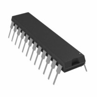
AD7870JNZ Analog Devices Inc, AD7870JNZ Datasheet - Page 12

AD7870JNZ
Manufacturer Part Number
AD7870JNZ
Description
IC ADC 12BIT LC2MOS 100KHZ 24DIP
Manufacturer
Analog Devices Inc
Datasheet
1.AD7870JNZ.pdf
(28 pages)
Specifications of AD7870JNZ
Data Interface
Serial, Parallel
Number Of Bits
12
Sampling Rate (per Second)
100k
Number Of Converters
1
Power Dissipation (max)
95mW
Voltage Supply Source
Dual ±
Operating Temperature
0°C ~ 70°C
Mounting Type
Through Hole
Package / Case
24-DIP (0.300", 7.62mm)
Resolution (bits)
12bit
Sampling Rate
100kSPS
Input Channel Type
Single Ended
Supply Voltage Range - Analog
± 4.75V To ± 5.25V
Supply Current
8mA
Number Of Elements
1
Resolution
12Bit
Architecture
SAR
Sample Rate
100KSPS
Input Polarity
Bipolar
Input Type
Voltage
Rated Input Volt
±3V
Differential Input
No
Power Supply Requirement
Dual
Single Supply Voltage (typ)
Not RequiredV
Single Supply Voltage (min)
Not RequiredV
Single Supply Voltage (max)
Not RequiredV
Dual Supply Voltage (typ)
±5V
Dual Supply Voltage (min)
±4.75V
Dual Supply Voltage (max)
±5.25V
Power Dissipation
95mW
Integral Nonlinearity Error
±0.5LSB(Typ)
Operating Temp Range
0C to 70C
Operating Temperature Classification
Commercial
Mounting
Through Hole
Pin Count
24
Package Type
PDIP
Input Signal Type
Single-Ended
Lead Free Status / RoHS Status
Lead free / RoHS Compliant
Lead Free Status / RoHS Status
Lead free / RoHS Compliant, Lead free / RoHS Compliant
AD7870/AD7875/AD7876
Figure 10 shows the analog input for the AD7875. The input
range is 0 V to +5 V into an input resistance of typically 25 kΩ.
Once again, the designed code transitions occur midway
between successive integer LSB values. The output code is
straight binary with 1 LSB = FS/4096 = 5 V/4096 = 1.22 mV.
The ideal input/output transfer function is shown in Figure 12.
REF OUT
AGND
OUTPUT
011…111
011…110
000…010
000…001
000…000
111…111
111…110
100…001
100…000
AGND
CODE
V
IN
V
IN
Figure 11. AD7870/AD7876 Transfer Function
7R
2R
AD7870 (AD7876)
2.1R
Figure 10. AD7875 Analog Input
–FS
Figure 9. AD7876 Analog Input
2
3R
3R
V
IN
TRACK-AND-HOLD
TRACK-AND-HOLD
– INPUT VOLTAGE
AD7875
TO INTERNAL AGND
TO INTERNAL
TO INTERNAL AGND
AD7876
REFERENCE
AMPLIFIER
AMPLIFIER
0V
COMPARATOR
TO INTERNAL
FS = 6V (20V)
1LSB =
COMPARATOR
TO INTERNAL
+FS – 1LSB
2
4096
FS
Rev. C | Page 12 of 28
OFFSET AND FULL-SCALE ADJUSTMENT—
AD7870
In most digital signal processing (DSP) applications, offset and
full-scale errors have little or no effect on system performance.
Offset error can always be eliminated in the analog domain
by ac coupling. Full-scale error effect is linear and does not
cause problems as long as the input signal is within the full
dynamic range of the ADC. Some applications will require
that the input signal span the full analog input dynamic range.
In such applications, offset and full-scale error have to be
adjusted to zero.
Where adjustment is required, offset error must be adjusted
before full-scale error. This is achieved by trimming the offset
of the op amp driving the analog input of the AD7870 while the
input voltage is 1/2 LSB below ground. The trim procedure is as
follows: apply a voltage of −0.73 mV(−1/2 LSB) at V
and adjust the op amp offset voltage until the ADC output code
flickers between 1111 1111 1111 and 0000 0000 0000. Gain
error can be adjusted at either the first code transition (ADC
negative full-scale) or the last code transition (ADC positive full
scale). The trim procedures for both cases are as follows (see
Figure 13).
OUTPUT
CODE
111…111
111…110
111…101
111…100
000…011
000…010
000…001
000…000
0V
Figure 12. AD7875 Transfer Function
V
IN
– INPUT VOLTAGE
FS = 5V
1LSB =
4096
FS
+FS – 1LSB
1
in Figure 13


