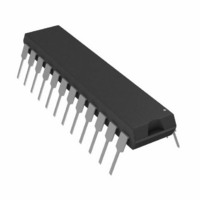
AD7870JNZ Analog Devices Inc, AD7870JNZ Datasheet - Page 3

AD7870JNZ
Manufacturer Part Number
AD7870JNZ
Description
IC ADC 12BIT LC2MOS 100KHZ 24DIP
Manufacturer
Analog Devices Inc
Datasheet
1.AD7870JNZ.pdf
(28 pages)
Specifications of AD7870JNZ
Data Interface
Serial, Parallel
Number Of Bits
12
Sampling Rate (per Second)
100k
Number Of Converters
1
Power Dissipation (max)
95mW
Voltage Supply Source
Dual ±
Operating Temperature
0°C ~ 70°C
Mounting Type
Through Hole
Package / Case
24-DIP (0.300", 7.62mm)
Resolution (bits)
12bit
Sampling Rate
100kSPS
Input Channel Type
Single Ended
Supply Voltage Range - Analog
± 4.75V To ± 5.25V
Supply Current
8mA
Number Of Elements
1
Resolution
12Bit
Architecture
SAR
Sample Rate
100KSPS
Input Polarity
Bipolar
Input Type
Voltage
Rated Input Volt
±3V
Differential Input
No
Power Supply Requirement
Dual
Single Supply Voltage (typ)
Not RequiredV
Single Supply Voltage (min)
Not RequiredV
Single Supply Voltage (max)
Not RequiredV
Dual Supply Voltage (typ)
±5V
Dual Supply Voltage (min)
±4.75V
Dual Supply Voltage (max)
±5.25V
Power Dissipation
95mW
Integral Nonlinearity Error
±0.5LSB(Typ)
Operating Temp Range
0C to 70C
Operating Temperature Classification
Commercial
Mounting
Through Hole
Pin Count
24
Package Type
PDIP
Input Signal Type
Single-Ended
Lead Free Status / RoHS Status
Lead free / RoHS Compliant
Lead Free Status / RoHS Status
Lead free / RoHS Compliant, Lead free / RoHS Compliant
SPECIFICATIONS
V
T
AD7870 SPECIFICATIONS
Table 1.
Parameter
DYNAMIC PERFORMANCE
DC ACCURACY
ANALOG INPUT
REFERENCE OUTPUT
LOGIC INPUTS
LOGIC OUTPUTS
max
DD
Signal-to-Noise Ratio
Total Harmonic Distortion (THD)
Peak Harmonic or Spurious Noise
Intermodulation Distortion (IMD)
Resolution
Minimum Resolution for which No Missing Codes
Integral Nonlinearity
Integral Nonlinearity
Differential Nonlinearity
Bipolar Zero Error
Positive Full-Scale Error
Negative Full-Scale Error
Input Voltage Range
Input Current
REF OUT @ +25°C
REF OUT Tempco
Reference Load Sensitivity
Input High Voltage, V
Input Low Voltage, V
Input Current, I
Input Current (12/8/CLK Input Only)
Input Capacitance, C
Output High Voltage, V
Output Low Voltage, V
DB11 to DB0
, unless otherwise noted.
= +5 V ± 5%, V
@ +25°C
T
Second Order Terms
Third Order Terms
Track-and-Hold Acquisition Time
are Guaranteed
(ΔREF OUT/ΔI)
Floating-State Leakage Current
Floating-State Output Capacitance
MIN
to T
MAX
IN
SS
= −5 V ± 5%, AGND = DGND = 0 V, f
3
INL
IN
INH
(SNR)
5
OL
OH
4
2
4
5
J, A
70
70
−80
−80
−80
−80
2
12
12
±1/2
±5
±5
±5
±3
±500
2.99
3.01
±60
±1
2.4
0.8
±10
±10
10
4.0
0.4
±10
15
CLK
K, B
70
70
−80
−80
−80
−80
2
12
12
±1/2
±1
±1
±5
±5
±5
±3
±500
2.99
3.01
±60
±1
2.4
0.8
±10
±10
10
4.0
0.4
±10
15
Rev. C | Page 3 of 28
ADN7870
= 2.5 MHz external, unless otherwise stated. All Specifications T
L, C
72
71
−80
−80
−80
−80
2
12
12
±1/4
±1/2
±1
±5
±5
±5
±3
±500
2.99
3.01
±35
±1
2.4
0.8
±10
±10
10
4.0
0.4
±10
15
1
T
69
69
−78
−78
−78
−78
2
12
±1
±5
±500
3.01
2.4
0.8
±10
±10
10
4.0
0.4
±10
15
12
±1/2
±1
±5
±5
±3
2.99
±35
±1
Units
dB min
dB min
dB max
dB max
dB max
dB max
μs max
Bits
Bits
LSB typ
LSB max
LSB max
LSB max
LSB max
LSB max
V
μA max
V min
V max
ppm/°C
max
mV max
V min
V max
μA max
μA max
pF max
V min
V max
μA max
pF max
Test Conditions/Comments
Typically 71.5 dB for 0 < V
V
Typically −86 dB for 0 < V
V
Typically −86 dB for 0 < V
fa = 9 kHz, fb = 9.5 kHz, f
fa = 9 kHz, fb = 9.5 kHz, f
Reference load current change (0 μA to
500 μA). Reference load should not be
changed during conversion.
V
V
V
V
I
I
V
SOURCE
SINK
AD7870/AD7875/AD7876
IN
IN
IN
DD
DD
IN
IN
= 10 kHz sine wave, f
= 10 kHz sine wave, f
= 10 kHz, f
= 0 V to V
= V
= 5 V ± 5%
= 5 V ± 5%
= 1.6 mA
= 40 μA
SS
to V
DD
DD
SAMPLE
= 100 kHz
SAMPLE
SAMPLE
SAMPLE
SAMPLE
IN
IN
IN
< 50 kHz
< 50 kHz
< 50 kHz
= 50 kHz
= 50 kHz
= 100 kHz
= 100 kHz
min
to


