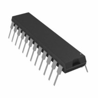
AD7870JNZ Analog Devices Inc, AD7870JNZ Datasheet - Page 21

AD7870JNZ
Manufacturer Part Number
AD7870JNZ
Description
IC ADC 12BIT LC2MOS 100KHZ 24DIP
Manufacturer
Analog Devices Inc
Datasheet
1.AD7870JNZ.pdf
(28 pages)
Specifications of AD7870JNZ
Data Interface
Serial, Parallel
Number Of Bits
12
Sampling Rate (per Second)
100k
Number Of Converters
1
Power Dissipation (max)
95mW
Voltage Supply Source
Dual ±
Operating Temperature
0°C ~ 70°C
Mounting Type
Through Hole
Package / Case
24-DIP (0.300", 7.62mm)
Resolution (bits)
12bit
Sampling Rate
100kSPS
Input Channel Type
Single Ended
Supply Voltage Range - Analog
± 4.75V To ± 5.25V
Supply Current
8mA
Number Of Elements
1
Resolution
12Bit
Architecture
SAR
Sample Rate
100KSPS
Input Polarity
Bipolar
Input Type
Voltage
Rated Input Volt
±3V
Differential Input
No
Power Supply Requirement
Dual
Single Supply Voltage (typ)
Not RequiredV
Single Supply Voltage (min)
Not RequiredV
Single Supply Voltage (max)
Not RequiredV
Dual Supply Voltage (typ)
±5V
Dual Supply Voltage (min)
±4.75V
Dual Supply Voltage (max)
±5.25V
Power Dissipation
95mW
Integral Nonlinearity Error
±0.5LSB(Typ)
Operating Temp Range
0C to 70C
Operating Temperature Classification
Commercial
Mounting
Through Hole
Pin Count
24
Package Type
PDIP
Input Signal Type
Single-Ended
Lead Free Status / RoHS Status
Lead free / RoHS Compliant
Lead Free Status / RoHS Status
Lead free / RoHS Compliant, Lead free / RoHS Compliant
TMS32020 Serial Interface
Figure 28 shows a serial interface between the AD7870/
AD7875/AD7876 and the TMS32020. The AD7870/AD7875/
AD7876 is configured for continuous clock operation. Note
that the ADC will not interface correctly to the TMS32020 if the
ADC is configured for a noncontinuous clock. Data is clocked
into the data receive register (DRR) of the TMS32020 during
conversion. As with the previous interfaces, when a 16-bit word
is received by the TMS32020 it generates an internal interrupt
to read the data from the DRR.
ADSP-2101/ADSP-2102 Serial Interface
Figure 29 shows a serial interface between the AD7870/
AD7875/AD7876 and the ADSP-2101/ADSP-2102. The ADC
is configured for continuous clock operation. Data is clocked
into the serial port register of the ADSP-2101/ADSP-2102
during conversion. As with the previous interfaces, when a 16-
bit data word is received by the ADSP-2101/ADSP-2102 an
internal microprocessor interrupt is generated and the data is
read from the serial port register.
1
ADDITIONAL PINS OMITTED FOR CLARITY.
TMS32020
CLKR
FSR
DR
Figure 28. TMS32020 Serial Interface
4.7kΩ
2kΩ
5V
TIMER
4.7kΩ
–5V
CONVST
12/8/CLK
SSTRB
SCLK
SDATA
AD7870/
AD7875/
AD7876
1
Rev. C | Page 21 of 28
STANDALONE OPERATION
The AD7870/AD7875/AD7876 can be used in its Mode 2,
parallel interface mode for standalone operation. In this case,
conversion is initiated with a pulse to the ADC CS input. This
pulse must be longer than the conversion time of the ADC. The
BUSY output is used to drive the RD input. Data is latched from
the ADC DB0–DB11 outputs to an external latch on the rising
edge of BUSY .
1
ADDITIONAL PINS OMITTED FOR CLARITY.
ADSP-2101/
ADSP-2102
CLKR
FSR
DR
Figure 29. ADSP-2101/ADSP-2102 Serial Interface
1
2
t
ADDITIONAL PINS OMITTED FOR CLARITY.
CS
4.7kΩ
LATCH
>
Figure 30. Stand-Alone Operation
t
CS
t
16
1
+
EN
2kΩ
t
CONVERT
+5V
AD7870/AD7875/AD7876
.
TIMER
4.7kΩ
RD
DB11
CS
BUSY
DB0
–5V
AD7870/
AD7875/
AD7876
SSTRB
SCLK
CONVST
12/8/CLK
SDATA
2
AD7870/
AD7875/
AD7876
1


