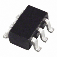
AD7466BRTZ-R2 Analog Devices Inc, AD7466BRTZ-R2 Datasheet - Page 10

AD7466BRTZ-R2
Manufacturer Part Number
AD7466BRTZ-R2
Description
IC ADC 12BIT 1.6V LP SOT23-6
Manufacturer
Analog Devices Inc
Specifications of AD7466BRTZ-R2
Data Interface
DSP, MICROWIRE™, QSPI™, Serial, SPI™
Design Resources
Software Calibrated, 50 MHz to 9 GHz, RF Power Measurement System (CN0178)
Number Of Bits
12
Sampling Rate (per Second)
200k
Number Of Converters
1
Power Dissipation (max)
900µW
Voltage Supply Source
Single Supply
Operating Temperature
-40°C ~ 85°C
Mounting Type
Surface Mount
Package / Case
SOT-23-6
Resolution (bits)
12bit
Sampling Rate
200kSPS
Input Channel Type
Single Ended
Supply Voltage Range - Analog
1.6V To 3.6V
Supply Current
300µA
Lead Free Status / RoHS Status
Lead free / RoHS Compliant
For Use With
EVAL-AD7466CBZ - BOARD EVALUATION FOR AD7466
Lead Free Status / RoHS Status
Lead free / RoHS Compliant, Lead free / RoHS Compliant
Available stocks
Company
Part Number
Manufacturer
Quantity
Price
Part Number:
AD7466BRTZ-R2
Manufacturer:
ADI/亚德诺
Quantity:
20 000
AD7466/AD7467/AD7468
TIMING EXAMPLES
Figure 3 and Figure 4 show some of the timing parameters from
the Timing Specifications section (Table 4).
Timing Example 1
As shown in Figure 4, f
100 kSPS gives a cycle time of t
Assuming V
4.41 µs = 4.46 µs, and t
satisfies the requirement of 10 ns for t
powered up and the signal is fully acquired at Point A. This
means that the acquisition/power-up time is t
55 ns + 588 ns = 643 ns, satisfying the maximum requirement of
640 ns for the power-up time.
SDATA
SCLK
SCLK
CS
THREE-STATE
CS
DD
= 1.8 V, t
POINT A: THE PART IF FULLY POWERED UP WITH V
t
t
2
2
ACQUISITION TIME
TRACK-AND-HOLD
8
SCLK
0
CONVERT
= 60 ns max, then t
1
1
t
3
IN TRACK
= 3.4 MHz and a throughput of
0
4 LEADING ZEROS
= t
CONVERT
2
2
2
B A
+ 15(1/f
0
QUIET
+ t
A
3
3
8
. The part is fully
+ t
t
SCLK
QUIET
4
0
Figure 3. AD7466 Serial Interface Timing Diagram Example
Figure 4. AD7466 Serial Interface Timing Diagram Example
QUIET
2
) = 55 ns +
+ 2(1/f
= 5.48 µs, which
4
4
DB11
= 10 µs.
t
6
t
CONVERT
SCLK
5
t
5
CONVERT
) =
t
DB10
7
IN
Rev. B | Page 10 of 28
FULLY ACQUIRED.
1/THROUGHPUT
TRACK-AND-HOLD IN HOLD
13
13
Timing Example 2
The AD7466 can also operate with slower clock frequencies.
As shown in Figure 4, assuming V
and a throughput of 50 kSPS gives a cycle time of t
t
7.55 µs, and t
which satisfies the requirement of 10 ns for t
fully powered up and the signal is fully acquired at Point A,
which means the acquisition/power-up time is t
55 ns + 1 µs = 1.05 µs, satisfying the maximum requirement of
640 ns for the power-up time. In this example and with other
slower clock values, the part is fully powered up and the signal
already acquired before the third SCLK falling edge; however,
the track-and-hold does not go into hold mode until that point.
In this example, the part can be powered up and the signal can
be fully acquired at approximately Point B in Figure 4.
DB2
QUIET
14
= 20 µs. With t
14
t
5
DB1
8
15
15
= 60 ns max, this leaves t
t
8
DB0
CONVERT
t
16
16
8
THREE-STATE
= t
POWER-DOWN
AUTOMATIC
2
+ 15(1/f
DD
t
t
QUIET
QUIET
= 1.8 V, f
t
1
QUIET
SCLK
) = 55 ns + 7.5 µs =
to be 12.39 µs,
QUIET
SCLK
2
. The part is
+ 2(1/f
= 2 MHz,
CONVERT
SCLK
+ t
) =
8
+


