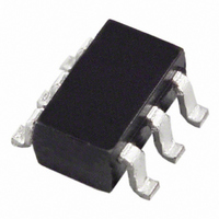
AD7466BRTZ-R2 Analog Devices Inc, AD7466BRTZ-R2 Datasheet - Page 23

AD7466BRTZ-R2
Manufacturer Part Number
AD7466BRTZ-R2
Description
IC ADC 12BIT 1.6V LP SOT23-6
Manufacturer
Analog Devices Inc
Specifications of AD7466BRTZ-R2
Data Interface
DSP, MICROWIRE™, QSPI™, Serial, SPI™
Design Resources
Software Calibrated, 50 MHz to 9 GHz, RF Power Measurement System (CN0178)
Number Of Bits
12
Sampling Rate (per Second)
200k
Number Of Converters
1
Power Dissipation (max)
900µW
Voltage Supply Source
Single Supply
Operating Temperature
-40°C ~ 85°C
Mounting Type
Surface Mount
Package / Case
SOT-23-6
Resolution (bits)
12bit
Sampling Rate
200kSPS
Input Channel Type
Single Ended
Supply Voltage Range - Analog
1.6V To 3.6V
Supply Current
300µA
Lead Free Status / RoHS Status
Lead free / RoHS Compliant
For Use With
EVAL-AD7466CBZ - BOARD EVALUATION FOR AD7466
Lead Free Status / RoHS Status
Lead free / RoHS Compliant, Lead free / RoHS Compliant
Available stocks
Company
Part Number
Manufacturer
Quantity
Price
Part Number:
AD7466BRTZ-R2
Manufacturer:
ADI/亚德诺
Quantity:
20 000
MICROPROCESSOR INTERFACING
The serial interface on the AD7466/AD7467/AD7468 allows
the parts to be connected directly to many different micro-
processors. This section explains how to interface the AD7466/
AD7467/AD7468 with some of the more common micro-
controller and DSP serial interface protocols.
AD7466/AD7467/AD7468 to TMS320C541 Interface
The serial interface on the TMS320C541 uses a continuous
serial clock and frame synchronization signals to synchronize
the data transfer operations with peripheral devices like the
AD7466/AD7467/AD7468. The CS input allows easy inter-
facing between the TMS320C541 and the AD74xx devices,
without requiring any glue logic. The serial port of the
TMS320C541 is set up to operate in burst mode (FSM = 1
in the serial port control register, SPC) with internal CLKX
(MCM = 1 in the SPC register) and internal frame signal
(TXM = 1 in the SPC register), so both pins are configured as
outputs. For the AD7466, the word length should be set to
16 bits (FO = 0 in the SPC register). The standard synchronous
serial port interface in this DSP allows only frames with a word
length of 16 bits or 8 bits. Therefore, for the AD7467 and
AD7468 where 14 and 12 bits are required, the FO bit also
would be set up to 16 bits. In these cases, the user should keep
in mind that the last 2 bits and 4 bits for the AD7467 and
AD7468, respectively, are invalid data as the SDATA line goes
back into three-state on the 14th and 12th SCLK falling edge.
To summarize, the values in the SPC register are FO = 0,
FSM = 1, MCM = 1, and TXM = 1.
Figure 33 shows the connection diagram. For signal processing
applications, it is imperative that the frame synchronization
signal from the TMS320C541 provide equidistant sampling.
1
ADDITIONAL PINS OMITTED FOR CLARITY.
SDATA
SCLK
AD7466/
AD7467/
AD7468
CS
THREE-STATE
Figure 33. Interfacing to the TMS320C541
SDATA
1
SCLK
CS
t
2
0
1
t
3
0
4 LEADING ZEROS
CLKX
CLKR
DR
FSX
FSR
2
TMS320C541
0
B
Figure 32. AD7468 Serial Interface Timing Diagram
3
1
0
4
t
CONVERT
Rev. B | Page 23 of 28
DB7
t
4
t
6
t
8 BITS OF DATA
5
t
7
AD7466/AD7467/AD7468 to ADSP-218x Interface
The ADSP-218x family of DSPs is interfaced directly to the
AD7466/AD7467/AD7468 without any glue logic. The SPORT
control register must be set up as described in Table 9.
Table 9. SPORT Control Register Setup
The connection diagram in Figure 34 shows how the
ADSP-218x has the TFS and RFS of the SPORT tied together,
with TFS set as an output and RFS set as an input. The DSP
operates in alternate framing mode, and the SPORT control
register is set up as described. The frame synchronization signal
generated on the TFS is tied to CS , and as with all signal proc-
essing applications, equidistant sampling is necessary. However,
in this example, the timer interrupt is used to control the sam-
pling rate of the ADC and, under certain conditions, equidistant
sampling might not be achieved.
The timer registers, for example, are loaded with a value that
provides an interrupt at the required sample interval. When an
interrupt is received, a value is transmitted with TFS/DT (ADC
control word). The TFS is used to control the RFS and, there-
fore, the reading of data. The frequency of the serial clock is set
in the SCLKDIV register. When the instruction to transmit with
TFS is given (that is, AX0 = TX0), the state of the SCLK is
checked. The DSP waits until the SCLK goes high, low, and high
again before transmission starts. If the timer and SCLK values
are chosen such that the instruction to transmit occurs on or
near the rising edge of SCLK, the data can be transmitted, or it
can wait until the next clock edge.
Setting
TFSW = RFSW = 1
INVRFS = INVTFS = 1
DTYPE = 00
ISCLK = 1
TFSR = RFSR = 1
IRFS = 0
ITFS = 1
SLEN = 1111
SLEN = 1101
SLEN = 1011
11
DB0
t
8
12
THREE-STATE
t
AD7466/AD7467/AD7468
QUIET
Description
Alternate framing
Active low frame signal
Right-justify data
Internal serial clock
Frame every word
Sets up RFS as an input
Sets up TFS as an output
16 bits for the AD7466
14 bits for the AD7467
12 bits for the AD7468
t
1


