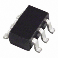
AD7466BRTZ-R2 Analog Devices Inc, AD7466BRTZ-R2 Datasheet - Page 22

AD7466BRTZ-R2
Manufacturer Part Number
AD7466BRTZ-R2
Description
IC ADC 12BIT 1.6V LP SOT23-6
Manufacturer
Analog Devices Inc
Specifications of AD7466BRTZ-R2
Data Interface
DSP, MICROWIRE™, QSPI™, Serial, SPI™
Design Resources
Software Calibrated, 50 MHz to 9 GHz, RF Power Measurement System (CN0178)
Number Of Bits
12
Sampling Rate (per Second)
200k
Number Of Converters
1
Power Dissipation (max)
900µW
Voltage Supply Source
Single Supply
Operating Temperature
-40°C ~ 85°C
Mounting Type
Surface Mount
Package / Case
SOT-23-6
Resolution (bits)
12bit
Sampling Rate
200kSPS
Input Channel Type
Single Ended
Supply Voltage Range - Analog
1.6V To 3.6V
Supply Current
300µA
Lead Free Status / RoHS Status
Lead free / RoHS Compliant
For Use With
EVAL-AD7466CBZ - BOARD EVALUATION FOR AD7466
Lead Free Status / RoHS Status
Lead free / RoHS Compliant, Lead free / RoHS Compliant
Available stocks
Company
Part Number
Manufacturer
Quantity
Price
Part Number:
AD7466BRTZ-R2
Manufacturer:
ADI/亚德诺
Quantity:
20 000
AD7466/AD7467/AD7468
SERIAL INTERFACE
Figure 30, Figure 31, and Figure 32 show the timing diagrams
for serial interfacing to the AD7466/AD7467/AD7468. The
serial clock provides the conversion clock and controls the
transfer of information from the ADC during a conversion.
The part begins to power up on the CS falling edge. The falling
edge of CS puts the track-and-hold into track mode and takes
the bus out of three-state. The conversion is also initiated at this
point. On the third SCLK falling edge after the CS falling edge,
the part should be powered-up fully at Point B, as shown in
Figure 30, and the track-and-hold returns to hold.
For the AD7466, the SDATA line goes back into three-state and
the part enters power-down on the 16th SCLK falling edge. If
the rising edge of CS occurs before 16 SCLKs elapse, the
conversion terminates, the SDATA line goes back into three-
state, and the part enters power-down; otherwise SDATA
returns to three-state on the 16th SCLK falling edge, as shown
in Figure 30. Sixteen serial clock cycles are required to perform
the conversion process and to access data from the AD7466.
For the AD7467, the 14th SCLK falling edge causes the SDATA
line to go back into three-state, and the part enters power-down.
If the rising edge of CS occurs before 14 SCLKs elapse, the con-
version terminates, the SDATA line goes back into three-state,
and the AD7467 enters power-down; otherwise SDATA returns
to three-state on the 14th SCLK falling edge, as shown in
Figure 31. Fourteen serial clock cycles are required to perform
the conversion process and to access data from the AD7467.
SDATA
SCLK
SDATA
SCLK
CS
THREE-STATE
CS
THREE-STATE
t
2
0
t
1
2
t
3
0
1
0
4 LEADING ZEROS
t
3
0
2
4 LEADING ZEROS
0
2
B
3
0
t
4
0
B
3
Figure 30. AD7466 Serial Interface Timing Diagram
Figure 31. AD7467 Serial Interface Timing Diagram
4
DB11
0
t
6
4
t
5
CONVERT
t
DB10
DB9
7
t
t
CONVERT
t
4
6
12 BITS OF DATA
Rev. B | Page 22 of 28
5
t
DB8
7
10 BITS OF DATA
13
DB2
For the AD7468, the 12th SCLK falling edge causes the SDATA
line to go back into three-state, and the part enters power-down.
If the rising edge of CS occurs before 12 SCLKs elapse, the con-
version terminates, the SDATA line goes back into three-state,
and the AD7468 enters power down; otherwise SDATA returns
to three-state on the 12th SCLK falling edge, as shown in
Figure 32. Twelve serial clock cycles are required to perform the
conversion process and to access data from the AD7468.
CS going low provides the first leading zero to be read in by the
microcontroller or DSP. The remaining data is then clocked out
by subsequent SCLK falling edges, beginning with the second
leading zero; thus, the first clock falling edge on the serial clock
has the first leading zero provided and also clocks out the
second leading zero. For the AD7466, the final bit in the data
transfer is valid on the 16th SCLK falling edge, having been
clocked out on the previous (15th) SCLK falling edge.
In applications with a slow SCLK, it is possible to read in data
on each SCLK rising edge. In such a case, the first falling edge of
SCLK after the CS falling edge clocks out the second leading
zero and can be read in the following rising edge. If the first
SCLK edge after the CS falling edge is a falling edge, the first
leading zero that was clocked out when CS went low is missed,
unless it is not read on the first SCLK falling edge. The 15th
falling edge of SCLK clocks out the last bit, and it can be read in
the following rising SCLK edge.
If the first SCLK edge after the CS falling edge is a rising edge,
CS clocks out the first leading zero, and it can be read on the
SCLK rising edge. The next SCLK falling edge clocks out the
second leading zero, and it can be read on the following rising
edge.
14
t
5
13
DB1
t
5
DB0
15
DB0
t
8
14
t
16
8
THREE-STATE
THREE-STATE
t
QUIET
t
QUIET
t
1
t
1


