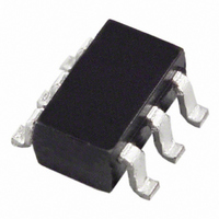
AD7466BRTZ-R2 Analog Devices Inc, AD7466BRTZ-R2 Datasheet - Page 9

AD7466BRTZ-R2
Manufacturer Part Number
AD7466BRTZ-R2
Description
IC ADC 12BIT 1.6V LP SOT23-6
Manufacturer
Analog Devices Inc
Specifications of AD7466BRTZ-R2
Data Interface
DSP, MICROWIRE™, QSPI™, Serial, SPI™
Design Resources
Software Calibrated, 50 MHz to 9 GHz, RF Power Measurement System (CN0178)
Number Of Bits
12
Sampling Rate (per Second)
200k
Number Of Converters
1
Power Dissipation (max)
900µW
Voltage Supply Source
Single Supply
Operating Temperature
-40°C ~ 85°C
Mounting Type
Surface Mount
Package / Case
SOT-23-6
Resolution (bits)
12bit
Sampling Rate
200kSPS
Input Channel Type
Single Ended
Supply Voltage Range - Analog
1.6V To 3.6V
Supply Current
300µA
Lead Free Status / RoHS Status
Lead free / RoHS Compliant
For Use With
EVAL-AD7466CBZ - BOARD EVALUATION FOR AD7466
Lead Free Status / RoHS Status
Lead free / RoHS Compliant, Lead free / RoHS Compliant
Available stocks
Company
Part Number
Manufacturer
Quantity
Price
Part Number:
AD7466BRTZ-R2
Manufacturer:
ADI/亚德诺
Quantity:
20 000
TIMING SPECIFICATIONS
For all devices, V
signals are specified with tr = tf = 5 ns (10% to 90% of V
Table 4.
Parameter
f
t
Acquisition Time
t
t
t
t
t
t
t
t
t
SCLK
CONVERT
QUIET
1
2
3
4
5
6
7
8
DD
= 1.6 V to 3.6 V; T
Limit at T
3.4
10
20
150
16 × t
12 × t
10 × t
780
640
10
10
55
55
140
0.4 t
0.4 t
10
60
7
SCLK
SCLK
SCLK
SCLK
SCLK
MIN
, T
MAX
A
= T
MIN
Figure 2. Load Circuit for Digital Output Timing Specifications
Unit
MHz max
kHz min
kHz min
kHz min
ns max
ns max
ns min
ns min
ns min
ns max
ns max
ns min
ns min
ns min
ns max
ns min
to T
MAX
TO OUTPUT
, unless otherwise noted. Sample tested at 25°C to ensure compliance. All input
DD
PIN
) and timed from a voltage level of 1.4 V.
Description
Mark/space ratio for the SCLK input is 40/60 to 60/40.
1.6 V ≤ V
V
V
AD7466.
AD7467.
AD7468.
Acquisition time/power-up time from power-down. See the Terminology
section. The acquisition time is the time required for the part to acquire a full-
scale step input value within ±1 LSB or a 30 kHz ac input value within ±0.5 LSB.
V
1.8 V ≤ V
Minimum quiet time required between bus relinquish and the start of the next
conversion.
Minimum CS pulse width.
CS to SCLK setup time. If V
minimum in order to meet the maximum figure for the acquisition time.
Delay from CS until SDATA is three-state disabled. Measured with the load
circuit in Figure 2 and defined as the time required for the output to cross the
V
Data access time after SCLK falling edge. Measured with the load circuit in
Figure 2 and defined as the time required for the output to cross the V
voltage.
SCLK low pulse width.
SCLK high pulse width.
SCLK to data valid hold time. Measured with the load circuit in Figure 2 and
defined as the time required for the output to cross the V
SCLK falling edge to SDATA three-state. t
taken by the data outputs to change 0.5 V when loaded with the circuit in
Figure 2. The measured number is then extrapolated back to remove the effects
of charging or discharging the 50 pF capacitor. This means that the time, t
quoted in the timing characteristics is the true bus relinquish time of the part,
and is independent of the bus loading.
SCLK falling edge to SDATA three-state.
DD
DD
DD
IH
50pF
Rev. B | Page 9 of 28
or V
= 3.3 V; minimum f
= 3.6 V; minimum f
= 1.6 V.
C
L
IL
200µA
200µA
DD
voltage.
DD
≤ 3 V; minimum f
≤ 3.6 V.
I
I
OL
OH
SCLK
SCLK
1.4V
DD
at which specifications are guaranteed.
at which specifications are guaranteed.
SCLK
= 1.6 V and f
at which specifications are guaranteed.
8
SCLK
is derived from the measured time
AD7466/AD7467/AD7468
= 3.4 MHz, t
2
IH
has to be 192 ns
or V
IL
voltage.
IH
or V
8
,
IL


