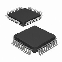
HI7188IN Intersil, HI7188IN Datasheet - Page 21

HI7188IN
Manufacturer Part Number
HI7188IN
Description
CONV A/D 16BIT 8:1 MUX 44-MQFP
Manufacturer
Intersil
Datasheet
1.HI7188IN.pdf
(24 pages)
Specifications of HI7188IN
Number Of Bits
16
Sampling Rate (per Second)
240
Data Interface
QSPI™, Serial, SPI™
Number Of Converters
1
Power Dissipation (max)
50mW
Voltage Supply Source
Analog and Digital, Dual ±
Operating Temperature
-40°C ~ 85°C
Mounting Type
Surface Mount
Package / Case
44-QFP
Lead Free Status / RoHS Status
Contains lead / RoHS non-compliant
Available stocks
Company
Part Number
Manufacturer
Quantity
Price
bipolar/unipolar operation. The 64 bits are divided into two 32
bit register blocks referred to as CCR#2 and CCR#1. Each
register contains four bytes pertaining to four logical channels.
The register may be accessed 1, 2, 3 or 4 bytes at a time.
Please refer to Table 10 to determine physical address
assignments within the CCR and Table 9 for logical channel
assignment. The physical channel conversion order is defined
based on it’s location in the CCR blocks. For example, if the
CCR #2 <31:24> is set with the CCR <2:0> = 100, then
physical channel 5 will be converted first. The CCR is byte wide
accessible via the Serial Interface allowing the user to change
the individual logical channel configuration on the fly. Following
are the bit assignments.
CH2, CH1, CH0 - Bits 7, 6, 5 of the channel configuration byte
determine which physical inputs are used as shown in Table 10.
B/U - Bit 4 of the channel configuration byte determine
bipolar or unipolar mode. If Logic 1, bipolar mode is selected
while logic 0 selects unipolar mode.
MD1, MD0 - Bit 3 and 2 of the channel configuration byte are
the channel Mode bits. This defines the mode of operation
for that logical channel, please see Table 11. All calibration
modes automatically return to conversion mode after
calibration is complete.
MSB
CH2
CH2, CH1, CH0 CCR [2:0]
BLOCK
CCR #2
CCR #2
CCR #2
CCR #2
CCR #1
CCR #1
CCR #1
CCR #1
TABLE 9. CHANNEL CONFIGURATION REGISTER
CHANNEL CONFIGURATION REGISTER (BYTE)
CH1
6
TABLE 10. ACTIVE CHANNEL DECODE
000
001
010
011
100
101
110
111
CH0
LOCATION
5
<31:24>
<23:16>
<31:24>
<23:16>
<15:8>
<15:8>
<7:0>
<7:0>
BIT
B/U
4
21
MD1
3
PHYSICAL INPUT PINS
2nd Logical Channel
3rd Logical Channel
1st Logical Channel
4th Logical Channel
5th Logical Channel
6th Logical Channel
7th Logical Channel
8th Logical Channel
DESCRIPTION
MD0
V
V
V
V
V
V
V
V
INH1
INH2
INH3
INH4
INH5
INH6
INH7
INH8
2
, V
, V
, V
, V
, V
, V
, V
, V
INL1
INL2
INL3
INL4
INL5
INL6
INL7
INL8
G1
1
LSB
G0
HI7188
G1, G0 - Bit 1 and 0 defines the PGIA gain of 1, 2, 4 or 8.
Please refer to Table 12.
Serial Interface Pin Description
The serial I/O port is a bidirectional port which is used to
read and write the internal registers. The port contains two
data lines, a synchronous clock, and two status flags.
Figure 14 shows a diagram of the serial interface lines.
SDO - Serial Data Out. Data is read from this line using those
protocols with separate lines for transmitting and receiving
data. An example of such a standard is the Motorola Serial
Peripheral Interface (SPI) using the 68HC05 and 68HC11
family of microcontrollers, or other similar processors. In the
case of using bidirectional data transfer on SDIO, the SDO
does not output data and is set in a high impedance state.
SDIO. Serial Data In or Out. Data is always written to the
device on this line. However, this line can be used as a
bidirectional data line. This is done by properly setting up the
Control Register. Bidirectional data transfer on this line can
be used with Intel standard serial interfaces (SSR, Mode 0)
in MCS51 and MCS96 family of microcontrollers, or other
similar processors.
SCLK. Serial Clock. The serial clock pin is used to
synchronize data to and from the HI7188 and to run the port
state machines. In Synchronous External Clock Mode, SCLK
is configured as an input, is supplied by the user, and can run
up to a 5MHz rate. In Synchronous Self Clocking Mode, SCLK
is configured as an output and runs at OSC
MD1
0
0
1
1
G1, G0 CCR [1:0]
BIDIRECTIONAL
END OF SCAN
CLOCK MODE
CALIBRATION
PORT CLOCK
CHIP SELECT
TABLE 11. HI7188 OPERATIONAL MODES
FIGURE 14. HI7188 SERIAL INTERFACE
DATA OUT
RESET I/O
MD0
00
01
10
11
ACTIVE
0
1
0
1
TABLE 12. CHANNEL GAIN
DATA
Conversion
System Offset Calibration
System Positive Full Scale Calibration
System Negative Full Scale Calibration
OPERATIONAL MODE
SDIO
SDO
SCLK
CS
EOS
CA
MODE
RSTI/O
PGIA CHANNEL GAIN
HI7188
1
/8 = 460.8kHz.
1
2
4
8


