HI7188IN Intersil, HI7188IN Datasheet - Page 6
HI7188IN
Manufacturer Part Number
HI7188IN
Description
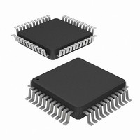
CONV A/D 16BIT 8:1 MUX 44-MQFP
Manufacturer
Intersil
Datasheet
1.HI7188IN.pdf
(24 pages)
Specifications of HI7188IN
Number Of Bits
16
Sampling Rate (per Second)
240
Data Interface
QSPI™, Serial, SPI™
Number Of Converters
1
Power Dissipation (max)
50mW
Voltage Supply Source
Analog and Digital, Dual ±
Operating Temperature
-40°C ~ 85°C
Mounting Type
Surface Mount
Package / Case
44-QFP
Lead Free Status / RoHS Status
Contains lead / RoHS non-compliant
Available stocks
Company
Part Number
Manufacturer
Quantity
Price


Absolute Maximum Ratings
Supply Voltage
Analog Input Pins. . . . . . . . . . . . . . . . . . . . . . . . . . . . AV
Digital Input, Output and I/O Pins . . . . . . . . . . . . . . DGND to DV
ESD Tolerance (No Damage)
Operating Conditions
Operating Temperature Range . . . . . . . . . . . . . . . . . -40
CAUTION: Stresses above those listed in “Absolute Maximum Ratings” may cause permanent damage to the device. This is a stress only rating and operation of the
device at these or any other conditions above those indicated in the operational sections of this specification is not implied.
NOTE:
Electrical Specifications
SYSTEM PERFORMANCE
Resolution
Integral Non-Linearity, INL
Differential Non-Linearity
Offset Error, V
Full Scale Error, FSE (Calibrated)
Gain Error (Calibrated)
Noise, V
Common Mode Rejection Ratio,
CMRR
Off Channel Isolation
ANALOG INPUT
Common Mode Input Range, V
Input Leakage Current, I
Input Capacitance, C
DIGITAL INPUTS
Input Logic High Voltage, V
Input Logic Low Voltage, V
Input Logic Current, I
Input Capacitance, C
DIGITAL CMOS OUTPUTS
Output Logic High Voltage, V
Output Logic Low Voltage, V
Output Three-State Leakage
Current, I
Digital Output Capacitance, C
1.
AV
DV
Human Body Model . . . . . . . . . . . . . . . . . . . . . . . . . . . . . . . .500V
Machine Model . . . . . . . . . . . . . . . . . . . . . . . . . . . . . . . . . . . .100V
Charged Device Model. . . . . . . . . . . . . . . . . . . . . . . . . . . . . .500V
DD
DD
JA
is measured with the component mounted on a low effective thermal conductivity test board in free air. See Tech Brief TB379 for details.
to AV
to DGND . . . . . . . . . . . . . . . . . . . . . . . . . . . . . . . . . . +5.5V
N(P-P)
OZ
SS
PARAMETER
OS
. . . . . . . . . . . . . . . . . . . . . . . . . . . . . . . . . . . . .11V
(Calibrated)
IN
I
IN
IN
IL
IH
OL
OH
OUT
CM
6
AV
OSC
DD
IN
= +5V, AV
= 3.6864MHz, Bipolar Input Range Selected
Dependent on Gain (Note 2)
F
End Point Line Method (Notes 3, 5, 6)
(Note 2)
V
V
Slope = +Full Scale - (-Full Scale)
(Notes 3, 4)
V
(Note 2)
(Note 2)
V
(Note 2) See Table 2
V
V
I
I
V
(Note 2)
OUT
OUT
S
INHI
INHI
CM
IN
IN
IN
OUT
= 25Hz, +FS, +MS, 0, -MS, -FS
= AV
= 0V, +5V
= 0V (Note 2)
= 0V (Note 5) Delta V
= -100 A (Note 7)
= 3.2mA (Note 7)
= V
- V
= 0V, +5V (Note 7)
SS
INLO
DD
INLO
= -5V, DV
SS
(Note 3)
o
TEST CONDITION
C to 85
= +2.5V (Notes 3, 4)
(Notes 3, 4)
to AV
DD
DD
DD
o
C
HI7188
= +5V, V
CM
= 3V
Thermal Information
Thermal Resistance (Typical, Note 1)
Maximum Storage Temperature Range . . . . . . . . . .-65
Maximum Junction Temperature . . . . . . . . . . . . . . . . . . . . . . . 150
Maximum Lead Temperature (Soldering 10s) . . . . . . . . . . . . . 300
RHI
MQFP . . . . . . . . . . . . . . . . . . . . . . . . . . . . . . . . . . .
(MQFP - Lead Tips Only)
= +2.5V, V
RLO
AV
-120
MIN
= AGND, V
2.0
2.4
-
-
-
-
-
-
-
-
-
-
-
-
-
-
-
No Missing Codes to 16-Bits
SS
-40
CM
o
C TO 85
0.0015
0.0015
0.0015
0.0015
TYP
1/4
-75
4.0
1.0
5.0
= AGND, PGIA Gain = 1,
10
1
-
-
-
-
-
-
-
-
o
C
0.0045
AV
MAX
1.0
0.8
0.4
16
10
10
-
-
-
-
-
-
-
-
-
-
-
DD
o
C to 150
JA
(
65
o
UNITS
C/W)
%FS
%FS
%FS
%FS
LSB
Bits
dB
dB
nA
pF
pF
pF
V
V
V
V
-
-
A
A
o
o
o
C
C
C
Related parts for HI7188IN
Image
Part Number
Description
Manufacturer
Datasheet
Request
R

Part Number:
Description:
8-channel, 16-bit, High Precision, Sigma-delta A/d Sub-system
Manufacturer:
Intersil Corporation
Datasheet:
Part Number:
Description:
Intersil Corporation [CMOS Serial Controller Interface]
Manufacturer:
Intersil Corporation
Datasheet:
Part Number:
Description:
Manufacturer:
Intersil Corporation
Datasheet:
Part Number:
Description:
357-036-542-201 CARDEDGE 36POS DL .156 BLK LOPRO
Manufacturer:
Intersil Corporation
Datasheet:
Part Number:
Description:
1024-Word x 4-Bit LSI Static RAM
Manufacturer:
Intersil Corporation
Datasheet:
Part Number:
Description:
General Purpose NPN Transistor Arrays FN341.4
Manufacturer:
Intersil Corporation
Datasheet:
Part Number:
Description:
CMOS 16-Bit Microprocessor
Manufacturer:
Intersil Corporation
Datasheet:
Part Number:
Description:
Manufacturer:
Intersil Corporation
Datasheet:
Part Number:
Description:
Manufacturer:
Intersil Corporation
Datasheet:
Part Number:
Description:
Manufacturer:
Intersil Corporation
Datasheet:
Part Number:
Description:
Manufacturer:
Intersil Corporation
Datasheet:
Part Number:
Description:
CMOS 6-Bit Latch and Decoder Memory Interfaces
Manufacturer:
Intersil Corporation
Datasheet:
Part Number:
Description:
CA3046General Purpose NPN Transistor Arrays
Manufacturer:
Intersil Corporation
Datasheet:
Part Number:
Description:
Manufacturer:
Intersil Corporation
Datasheet:
Part Number:
Description:
TR909 DLC/FLC SLIC with Low Power Standby
Manufacturer:
Intersil Corporation
Datasheet: