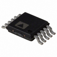
AD5627BRMZ Analog Devices Inc, AD5627BRMZ Datasheet - Page 20

AD5627BRMZ
Manufacturer Part Number
AD5627BRMZ
Description
IC DAC NANO 12BIT DUAL 10-MSOP
Manufacturer
Analog Devices Inc
Series
nanoDAC™r
Datasheet
1.AD5627RBCPZ-REEL7.pdf
(32 pages)
Specifications of AD5627BRMZ
Data Interface
Serial
Settling Time
3µs
Number Of Bits
12
Number Of Converters
2
Voltage Supply Source
Single Supply
Power Dissipation (max)
5.75mW
Operating Temperature
-40°C ~ 105°C
Mounting Type
Surface Mount
Package / Case
10-MSOP, Micro10™, 10-uMAX, 10-uSOP
Resolution (bits)
12bit
Sampling Rate
333kSPS
Input Channel Type
Serial
Supply Voltage Range - Analog
2.7V To 5.5V
Supply Current
950µA
Digital Ic Case Style
SOP
Lead Free Status / RoHS Status
Lead free / RoHS Compliant
Available stocks
Company
Part Number
Manufacturer
Quantity
Price
Company:
Part Number:
AD5627BRMZ
Manufacturer:
ADI
Quantity:
184
AD5627R/AD5647R/AD5667R, AD5627/AD5667
THEORY OF OPERATION
D/A SECTION
The AD56x7R/AD56x7 DACs are fabricated on a CMOS
process. The architecture consists of a string DAC followed by
an output buffer amplifier. Figure 52 shows a block diagram of
the DAC architecture.
Because the input coding to the DAC is straight binary, the ideal
output voltage when using an external reference is given by
The ideal output voltage when using the internal reference is
given by
where:
D is the decimal equivalent of the binary code that is loaded to
the DAC register:
N is the DAC resolution.
RESISTOR STRING
The resistor string is shown in Figure 53. It is simply a string of
resistors, each of value R. The code loaded to the DAC register
determines at which node on the string the voltage is tapped off
to be fed into the output amplifier. The voltage is tapped off by
closing one of the switches connecting the string to the amplifier.
Because it is a string of resistors, it is guaranteed monotonic.
OUTPUT AMPLIFIER
The output buffer amplifier can generate rail-to-rail voltages on
its output, which gives an output range of 0 V to V
a load of 2 kΩ in parallel with 1000 pF to GND. The source and
sink capabilities of the output amplifier can be seen in Figure 33
and Figure 34. The slew rate is 1.8 V/μs with a ¼ to ¾ full-scale
settling time of 7 μs.
0 to 4095 for AD5627R/AD5627 (12-bit).
0 to 16,383 for AD5647R (14-bit).
0 to 65,535 for AD5667R/AD5667 (16-bit).
V
V
OUT
OUT
REGISTER
=
=
DAC
V
2
REFIN
×
V
REFOUT
×
Figure 52. DAC Architecture
⎛
⎜
⎝
2
D
×
N
RESISTOR
⎞
⎟
⎠
⎛
⎜
⎝
STRING
REF (+)
REF (–)
2
GND
D
V
N
DD
⎞
⎟
⎠
OUTPUT
AMPLIFIER
GAIN = +2
DD
V
OUT
. It can drive
Rev. 0 | Page 20 of 32
INTERNAL REFERENCE
The AD5627R/AD5647R/AD5667R feature an on-chip
reference. Versions without the R suffix require an external
reference. The on-chip reference is off at power-up and is
enabled via a write to a control register. See the Internal
Reference Setup section for details.
Versions packaged in a 10-lead LFCSP package have a 1.25 V
reference, giving a full-scale output of 2.5 V. These parts can be
operated with a V
in a 10-lead MSOP package have a 2.5 V reference, giving a full-
scale output of 5 V. The parts are functional with a V
of 2.7 V to 5.5 V, but with a V
output is clamped to V
of models. The internal reference associated with each part is
available at the V
A buffer is required if the reference output is used to drive
external loads. When using the internal reference, it is
recommended that a 100 nF capacitor be placed between the
reference output and GND for reference stability.
EXTERNAL REFERENCE
The AD5627/AD5667 require an external reference, which is
applied at the V
the use of an external reference if the application requires it.
The default condition of the on-chip reference is off at power-
up. All devices can be operated from a single 2.7 V to 5.5 V supply.
R
R
R
R
R
REFIN
REFOUT
DD
supply of 2.7 V to 5.5 V. Versions packaged
pin. The V
Figure 53. Resistor String
DD
pin.
. See the Ordering Guide for a full list
DD
REFIN
supply of less than 5 V, the
pin on the AD56x7R allows
TO OUTPUT
AMPLIFIER
DD
supply


