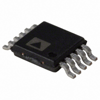
AD5627BRMZ Analog Devices Inc, AD5627BRMZ Datasheet - Page 7

AD5627BRMZ
Manufacturer Part Number
AD5627BRMZ
Description
IC DAC NANO 12BIT DUAL 10-MSOP
Manufacturer
Analog Devices Inc
Series
nanoDAC™r
Datasheet
1.AD5627RBCPZ-REEL7.pdf
(32 pages)
Specifications of AD5627BRMZ
Data Interface
Serial
Settling Time
3µs
Number Of Bits
12
Number Of Converters
2
Voltage Supply Source
Single Supply
Power Dissipation (max)
5.75mW
Operating Temperature
-40°C ~ 105°C
Mounting Type
Surface Mount
Package / Case
10-MSOP, Micro10™, 10-uMAX, 10-uSOP
Resolution (bits)
12bit
Sampling Rate
333kSPS
Input Channel Type
Serial
Supply Voltage Range - Analog
2.7V To 5.5V
Supply Current
950µA
Digital Ic Case Style
SOP
Lead Free Status / RoHS Status
Lead free / RoHS Compliant
Available stocks
Company
Part Number
Manufacturer
Quantity
Price
Company:
Part Number:
AD5627BRMZ
Manufacturer:
ADI
Quantity:
184
Parameter
t
t
t
t
t
1
2
3
4
12
13
14
15
SP
See Figure 3. High speed mode timing specification applies only to the AD5627RBRMZ-2/AD5627BRMZ-2REEL7 and AD5667RBRMZ-2/AD5667BRMZ-2REEL7.
CB refers to the capacitance on the bus line.
The SDA and SCL timing is measured with the input filters enabled. Switching off the input filters improves the transfer rate but has a negative effect on EMC behavior
of the part.
Input filtering on the SCL and SDA inputs suppresses noise spikes that are less than 50 ns for fast mode or 10 ns for high speed mode.
4
LDAC*
CLR
SDA
SCL
Conditions
Standard mode
Fast mode
High speed mode, C
High speed mode, C
Standard mode
Fast mode
High speed mode
Standard mode
Fast mode
High speed mode
Standard mode
Fast mode
High speed mode
Fast mode
High speed mode
*ASYNCHRONOUS LDAC UPDATE MODE.
P
t
7
S
2
t
t
6
2
B
B
= 100 pF
= 400 pF
t
4
t
11
Min
10
20
10
10
10
300
300
30
20
20
20
0
0
Figure 3. 2-Wire Serial Interface Timing Diagram
Max
300
300
40
80
50
10
t
3
t
1
t
12
Rev. 0 | Page 7 of 32
Unit
ns
ns
ns
ns
ns
ns
ns
ns
ns
ns
ns
ns
ns
ns
ns
AD5627R/AD5647R/AD5667R, AD5627/AD5667
t
15
Description
t
LDAC pulse width low
Falling edge of 9
falling edge
CLR pulse width low
Pulse width of spike suppressed
FCL
, fall time of SCL signal
S
t
t
5
10
t
6
th
SCL clock pulse of last byte of valid write to LDAC
t
14
t
8
t
13
P
t
9


