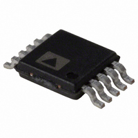
AD5627BRMZ Analog Devices Inc, AD5627BRMZ Datasheet - Page 26

AD5627BRMZ
Manufacturer Part Number
AD5627BRMZ
Description
IC DAC NANO 12BIT DUAL 10-MSOP
Manufacturer
Analog Devices Inc
Series
nanoDAC™r
Datasheet
1.AD5627RBCPZ-REEL7.pdf
(32 pages)
Specifications of AD5627BRMZ
Data Interface
Serial
Settling Time
3µs
Number Of Bits
12
Number Of Converters
2
Voltage Supply Source
Single Supply
Power Dissipation (max)
5.75mW
Operating Temperature
-40°C ~ 105°C
Mounting Type
Surface Mount
Package / Case
10-MSOP, Micro10™, 10-uMAX, 10-uSOP
Resolution (bits)
12bit
Sampling Rate
333kSPS
Input Channel Type
Serial
Supply Voltage Range - Analog
2.7V To 5.5V
Supply Current
950µA
Digital Ic Case Style
SOP
Lead Free Status / RoHS Status
Lead free / RoHS Compliant
Available stocks
Company
Part Number
Manufacturer
Quantity
Price
Company:
Part Number:
AD5627BRMZ
Manufacturer:
ADI
Quantity:
184
AD5627R/AD5647R/AD5667R, AD5627/AD5667
POWER-ON RESET AND SOFTWARE RESET
The AD56x7R/AD56x7 contain a power-on reset circuit that
controls the output voltage during power-up. The device powers
up to 0 V and the output remains powered up at this level until
a valid write sequence is made to the DAC. This is useful in
applications where it is important to know the state of the
output of the DAC while it is in the process of powering up. Any
events on LDAC or CLR during power-on reset are ignored.
There is also a software reset function. Command 101 is the
software reset command. The software reset command contains
two reset modes that are software programmable by setting Bit
DB0 in the input shift register.
Table 12 shows how the state of the bit corresponds to the
software reset modes of operation of the devices. Figure 64
shows the contents of the input shift register during the
software reset mode of operation.
Table 12. Software Reset Modes for the AD56x7R/AD56x7
DB0
0
1 (Power-On Reset)
R
0
R
X
0
0
S
X
S
X
S
X
C2
1
C2
C2
1
1
COMMAND
COMMAND
COMMAND
C1
0
C1
C1
0
1
C0
0
Registers reset to zero
DAC register
Input shift register
DAC register
Input shift register
LDAC register
Power-down register
Internal reference setup register
C0
C0
1
1
A2
X
DAC ADDRESS
(DON’T CARE)
A2
A2
X
X
DAC ADDRESS
DAC ADDRESS
(DON’T CARE)
(DON’T CARE)
A1
X
A1
A1
X
X
A0
X
A0
A0
X
X
DB15 DB14 DB13 DB12 DB11 DB10
DB15 DB14 DB13 DB12 DB11 DB10
DB15 DB14 DB13 DB12 DB11 DB10
X
X
X
X
Figure 65. Power Up/Down Command
Figure 66. Reference Setup Command
X
Figure 64. Software Reset Command
X
X
X
X
Rev. 0 | Page 26 of 32
DON’T CARE
DON’T CARE
DON’T CARE
X
X
X
X
X
X
CLEAR PIN (CLR)
The AD56x7R/AD56x7 has an asynchronous clear input. The
CLR input is falling-edge sensitive. While CLR is low, all LDAC
pulses are ignored. When CLR is activated, zero scale is loaded
to all input and DAC registers. This clears the output to 0 V. The
part exits clear code mode on the on the falling edge of the 9
clock pulse of the last byte of valid write. If CLR is activated
during a write sequence, the write is aborted. If CLR is activated
during high speed mode, the part exits high speed mode to
standard/fast mode.
INTERNAL REFERENCE SETUP (R VERSIONS)
The on-chip reference is off at power-up by default. It can be
turned on by sending the reference setup command (111) and
setting DB0 in the input shift register. Table 13 shows how the
state of the bit corresponds to the mode of operation. See Figure 66
for the contents of the input shift register during the internal
reference setup command.
Table 13. Reference Setup Command
DB0
0
1
X
X
X
DB9
X
DB9
DB9
X
X
DB8
X
DB8
DB8
X
X
Action
Internal reference off (default)
Internal reference on
DON’T CARE
DB7
X
DB7
DB7
X
X
DB6
X
DB6
DB6
X
X
DOWN MODE DON’T CARE
DB5
PD1
POWER-
DB5
DB5
X
X
DON’T CARE
DON’T CARE
DB4
PD0
DB4
DB4
X
X
DB3
X
DB3
DB3
X
X
DB2
X
DB2
DB2
(1 = DAC SELECTED)
X
X
DACB DACA
DAC SELECT
DB1
DB1
DB1
X
X
DB0
DB0
RST
DB0
REF
th


