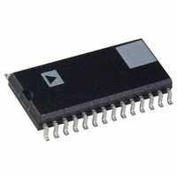
ADMCF326BRZ Analog Devices Inc, ADMCF326BRZ Datasheet - Page 17

ADMCF326BRZ
Manufacturer Part Number
ADMCF326BRZ
Description
IC DSP FLASH MOTOR CTRLR 28SOIC
Manufacturer
Analog Devices Inc
Series
Motor Controlr
Type
Fixed Pointr
Datasheet
1.ADMCF326BN.pdf
(36 pages)
Specifications of ADMCF326BRZ
Interface
Synchronous Serial Port (SSP)
Clock Rate
20MHz
Non-volatile Memory
FLASH (12 kB), ROM (12kB)
On-chip Ram
2.5kB
Voltage - I/o
5.00V
Voltage - Core
5.00V
Operating Temperature
-40°C ~ 85°C
Mounting Type
Surface Mount
Package / Case
28-SOIC (7.5mm Width)
Lead Free Status / RoHS Status
Lead free / RoHS Compliant
Available stocks
Company
Part Number
Manufacturer
Quantity
Price
Company:
Part Number:
ADMCF326BRZ
Manufacturer:
SHARP
Quantity:
1 000
Part Number:
ADMCF326BRZ
Manufacturer:
ADI/亚德诺
Quantity:
20 000
16-BIT PWM TIMER
Parameter
Counter Resolution
Edge Resolution (Single Update Mode)
Edge Resolution (Double Update Mode)
Programmable Dead Time Range
Programmable Dead Time Increments
Programmable Pulse Deletion Range
Programmable Pulse Deletion Increments
PWM Frequency Range
PWMSYNC Pulsewidth (T
Gate Drive Chop Frequency Range
Restarting the PWM after a fault condition is detected requires
clearing the fault and reinitializing the PWM. Clearing the fault
requires that PWMTRIP returns to a HI state. After the fault has
been cleared, the PWM can be restarted by writing to registers
PWMTM, PWMCHA, PWMCHB, and PWMCHC. After the fault
is cleared and the PWM registers are initialized, internal timing of
the three-phase timing unit will resume, and the new duty cycle
values will be latched on the next rising edge of PWMSYNC.
PWM Registers
The configuration of the PWM registers is described at the end
of the data sheet. The parameters of the PWM block are tabu-
lated in Table V.
ADC OVERVIEW
The ADC of the ADMCF326 is based upon the single slope
conversion technique. This approach offers an inherently
monotonic conversion process within the noise and stability of its
components, and there will be no missing codes.
Select
VAUX0
VAUX1
VAUX2
Calibration (V
The single slope technique has been adapted on the ADMCF326
for four channels that are simultaneously converted. Refer to
Figure 11 for the functional schematic of the ADC. Three of
the main inputs (V1, V2, and V3) are directly connected as
high impedance voltage inputs. The fourth channel has been con-
figured with a serially-connected 4-to-1 multiplexer. Table VI
shows the multiplexer input selection codes. One of these auxil-
iary multiplexed channels is used to calibrate the ramp against the
internal voltage reference (V
REV. B
Table VI. ADC Auxiliary Channel Selection
REF
)
Table V. Fundamental Characteristics of PWM Generation Unit of ADMCF326
MODECTRL (1)
ADCMUX1
REF
CRST
0
0
1
1
).
)
MODECTRL (0)
ADCMUX0
0
1
0
1
–17–
Comparing each ADC input to a reference ramp voltage and
timing the comparison of the two signals performs the conversion
process. The actual conversion point is the time point inter-
section of the input voltage and the ramp voltage (V
Figure 12. This time is converted to counts by the 12-bit ADC
Timer Block and is stored in the ADC registers. The ramp voltage
used to perform the conversion is generated by driving a fixed
current into an off-chip capacitor, where the capacitor voltage is
Following reset, V
the conversion process are initiated by the PWMSYNC pulse,
as shown in Figure 12. The width of the PWMSYNC pulse is
controlled by the PWMSYNCWT Register and should be pro-
grammed according to Figure 13 to ensure complete resetting.
In order to compensate for IC process manufacturing tolerances
(and to adjust for capacitor tolerances), the current source of the
ADMCF326 is software programmable. The software setting of the
magnitude of the ICONST current generator is accomplished by
selecting one of eight steps over approximately 20% current range.
C
GND
EXTERNAL
CHARGING
CAP
ICONST
VAUX2
VAUX0
VAUX1
V2
V3
V1
Min
0
150
0.05
0.02
V
C
Figure 11. ADC Overview
C
= 0 at t = 0. This reset and the start of
MUX
4–1
V
C
Typ
16
100
50
100
0
100
COMP
COMP
VREF
=
COMP
COMP
(
ICONST_TRIM<2:0>
I C
(CAP RESET)
)
×
V1L
V2L
V3L
VAUXL
t
Max
100
100
12.5
5
BLOCK
REGISTERS
12-BIT
TIMER
ADC
ADMCF326
ADC
PWMSYNC (CONVST)
CLK MODECTRL<7>
C
Unit
Bits
ns
ns
µs
ns
µs
ns
Hz
µs
MHz
) as shown in
ADC REGISTERS
ADC1
ADC2
ADC3
ADCAUX
MODECTRL<0..1>


