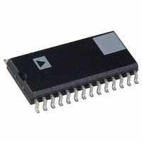
ADMCF326BRZ Analog Devices Inc, ADMCF326BRZ Datasheet - Page 7

ADMCF326BRZ
Manufacturer Part Number
ADMCF326BRZ
Description
IC DSP FLASH MOTOR CTRLR 28SOIC
Manufacturer
Analog Devices Inc
Series
Motor Controlr
Type
Fixed Pointr
Datasheet
1.ADMCF326BN.pdf
(36 pages)
Specifications of ADMCF326BRZ
Interface
Synchronous Serial Port (SSP)
Clock Rate
20MHz
Non-volatile Memory
FLASH (12 kB), ROM (12kB)
On-chip Ram
2.5kB
Voltage - I/o
5.00V
Voltage - Core
5.00V
Operating Temperature
-40°C ~ 85°C
Mounting Type
Surface Mount
Package / Case
28-SOIC (7.5mm Width)
Lead Free Status / RoHS Status
Lead free / RoHS Compliant
Available stocks
Company
Part Number
Manufacturer
Quantity
Price
Company:
Part Number:
ADMCF326BRZ
Manufacturer:
SHARP
Quantity:
1 000
Part Number:
ADMCF326BRZ
Manufacturer:
ADI/亚德诺
Quantity:
20 000
GENERAL DESCRIPTION
The ADMCF326 is a low cost, single-chip DSP-based controller,
suitable for permanent magnet synchronous motors, ac induction
motors, and brushless dc motors. The ADMCF326 integrates a
20 MIPS, fixed-point DSP core with a complete set of motor
control and system peripherals that permits fast, efficient devel-
opment of motor controllers.
The DSP core of the ADMCF326 is the ADSP-2171, which is
completely code-compatible with the ADSP-21xx DSP family
and combines three computational units, data address generators
and a program sequencer. The computational units comprise an
ALU, a multiplier/accumulator (MAC), and a barrel shifter.
The ADSP-2171 adds new instructions for bit manipulation,
multiplication (× squared), biased rounding, and global inter-
rupt masking.
The system peripherals are the power-on reset circuit (POR),
the watchdog timer and a synchronous serial port. The serial
port is configurable and double buffered, with hardware support
for UART and SCI port emulation.
The ADMCF326 provides 512 × 24-bit program memory RAM,
4K × 24-bit program memory ROM, 4K × 24-bit program
REV. B
OUTPUT REGS
INPUT REGS
GENERATOR
ADDRESS
DATA
ALU
#1
GENERATOR
ADDRESS
DATA
#2
OUTPUT REGS
INPUT REGS
MAC
16
R BUS
SEQUENCER
INSTRUCTION
PROGRAM
REGISTER
Figure 3. DSP Core Block Diagram
OUTPUT REGS
INPUT REGS
EXCHANGE
SHIFTER
BUS
14
14
24
16
–7–
FLASH memory, and 512 × 16-bit data memory RAM. The
user code will be stored and executed from the flash memory.
The program and data memory RAM can be used for dynamic
data storage or can be loaded through the serial port from an
external device as in other ADMCxxx family parts. The program
memory ROM contains a monitor function as well as useful rou-
tines for erasing, programming, and verifying the flash memory.
The motor control peripherals of the ADMCF326 provide a 12-bit
analog data acquisition system with six analog input channels,
and an internal voltage reference. In addition, a three-phase,
16-bit, center-based PWM generation unit can be used to produce
high accuracy PWM signals with minimal processor overhead.
The ADMCF326 also contains two auxiliary PWM outputs
and nine lines of digital I/O.
Because the ADMCF326 has a limited number of pins, functions
such as the auxiliary PWM and the serial communication port
are multiplexed with the nine programmable input/output (PIO)
pins. The pin functions can be independently selected to allow
maximum flexibility for different applications.
512
PM ROM
PM RAM
4K
CONTROL
LOGIC
24
24
COMPANDING
CIRCUITRY
PMA BUS
DMA BUS
PMD BUS
DMD BUS
PROGRAM
MEMORY
4K
FLASH
24
TRANSMIT REG
RECEIVE REG
SERIAL
6
PORT
ADMCF326
TIMER
512
DM RAM
16


