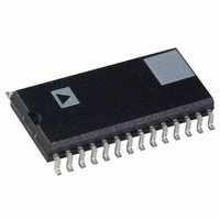
ADMCF326BRZ Analog Devices Inc, ADMCF326BRZ Datasheet - Page 22

ADMCF326BRZ
Manufacturer Part Number
ADMCF326BRZ
Description
IC DSP FLASH MOTOR CTRLR 28SOIC
Manufacturer
Analog Devices Inc
Series
Motor Controlr
Type
Fixed Pointr
Datasheet
1.ADMCF326BN.pdf
(36 pages)
Specifications of ADMCF326BRZ
Interface
Synchronous Serial Port (SSP)
Clock Rate
20MHz
Non-volatile Memory
FLASH (12 kB), ROM (12kB)
On-chip Ram
2.5kB
Voltage - I/o
5.00V
Voltage - Core
5.00V
Operating Temperature
-40°C ~ 85°C
Mounting Type
Surface Mount
Package / Case
28-SOIC (7.5mm Width)
Lead Free Status / RoHS Status
Lead free / RoHS Compliant
Available stocks
Company
Part Number
Manufacturer
Quantity
Price
Company:
Part Number:
ADMCF326BRZ
Manufacturer:
SHARP
Quantity:
1 000
Part Number:
ADMCF326BRZ
Manufacturer:
ADI/亚德诺
Quantity:
20 000
ADMCF326
Bit 2 is used to configure the IRQ2 interrupt. It is recommended
that the IRQ2 interrupt always be configured as level-sensitive
to ensure that no peripheral interrupts are lost. Setting Bit 4 of
the ICNTL Register enables interrupt nesting. The configura-
tion of both the IFC and ICNTL Registers is shown at the end
of the data sheet.
Interrupt Operation
Following a reset, the ROM code on the ADMCF326 must
copy a default interrupt vector table into program memory
RAM from Address 0x0000 to 0x002F. Since each interrupt
source has a dedicated four-word space in this vector table, it is
possible to code short interrupt service routines (ISR) in place.
Alternatively, it may be necessary to insert a JUMP instruction
to the appropriate start address of the interrupt service routine if
more memory is required for the ISR.
When an interrupt occurs, the program sequencer ensures that
there is no latency (beyond synchronization delay) when pro-
cessing unmasked interrupts. In the case of the timer, SPORT1,
and software interrupts, the interrupt controller automatically
jumps to the appropriate location in the interrupt vector table. At
this point, a JUMP instruction to the appropriate ISR is required.
Motor control peripheral interrupts are slightly different. When a
peripheral interrupt is detected, a bit is set in the IRQFLAG Regis-
ter for PWMSYNC and PWMTRIP, or in the PIOFLAG0 or
PIOFLAG1 Registers for a PIO interrupt, and the IRQ2 line
is pulled low until all pending interrupts are acknowledged.
The DSP software must determine the source of the interrupts
by reading IRQFLAG Register. If more than one interrupt
occurs simultaneously, the higher priority interrupt service routine
is executed. Reading the IRQFLAG Register clears the PWMTRIP
and PWMSYNC bits and acknowledges the interrupt, thus allow-
ing further interrupts when the ISR exits.
A user’s PIO interrupt service routine must read the PIOFLAG0
and PIOFLAG1 Registers to determine which PIO port is
the source of the interrupt. Reading registers PIOFLAG0 and
PIOFLAG1 clears all bits in the registers and acknowledges
the interrupt, thus allowing further interrupts after the ISR exits.
The configuration of all these registers is shown at the end of
the data sheet.
SYSTEM CONTROLLER
The system controller block of the ADMCF326 performs the
following functions:
1. Manages the interface and data transfer between the DSP core
2. Handles interrupts generated by the motor control peripherals
3. Controls the ADC multiplexer select lines
4. Enables PWMTRIP and PWMSYNC interrupts
5. Controls the multiplexing of the SPORT1 pins to select either
6. Controls the PWM Single/Double Update Mode
7. Controls the ADC conversion time modes
8. Controls the auxiliary PWM Operation Mode
and the motor control peripherals
and generates a DSP core interrupt signal IRQ2
DR1A or DR1B data receive pins. It also allows configura-
tion of SPORT1 as a UART interface.
–22–
9. Contains a status register (SYSSTAT) that indicates the state
10. Performs a reset of the motor control peripherals and control
SPORT1 Control
Both data receive pins are multiplexed internally into the single
data receive input of SPORT1 as shown in Figure 18. Two con-
trol bits in the MODECTRL Register control the state of the
SPORT1 pins by manipulating internal multiplexers in the
ADMCF326.
Bit 4 of the MODECTRL Register (DR1SEL) selects between the
two data receive pins. Setting Bit 4 of MODECTRL connects pin
DR1B to the internal data receive port DR1 of SPORT1. Clearing
Bit 4 connects DR1A to DR1.
Setting Bit 5 of the MODECTRL Register (SPORT1 Mode) con-
figures the serial port for UART Mode. In this mode, the DR1 and
RFS1 pins of the internal serial port are connected together. Addi-
tionally, setting the SPORT1 Mode bit connects the FL1 flag of
the DSP to the external PIO5/RFS1 pin.
Flag Pins
The ADMCF326 provides flag pins. The alternate configuration
of SPORT1 includes a Flag In (FI) and Flag Out (FO) pin.
This alternate configuration of SPORT1 is selected by Bit 10 of
the DSP system control register, SYSCNTL at data memory
address 0x3FFF. In the alternate configuration, the DR1 pin
(either DR1A or DR1B depending upon the state of the DR1SEL
bit) becomes the FI pin and the DT1 pin becomes the FO pin.
Additionally, RFS1 is configured as the IRQ0 interrupt input
and TFS1 is configured as the IRQ1 interrupt. The serial port
clock, SCLK1, is still available in the alternate configuration.
Development Tools
Users are recommended to obtain the ADMCF326-EVALKIT
from Analog Devices. The tool kit contains everything required
to quickly and easily evaluate and develop applications using the
ADMCF326 and ADMC326 DSP Motor Controllers. Please
contact your ADI sales representative for ordering information.
of the PWMTRIP pin, the watchdog timer, and the PWM
timer
registers following a hardware, software, or watchdog initi-
ated reset
DSP
CORE
SPORT1
Figure 18. Internal Multiplexing of SPORT1 Pins
SCLK1
RFS1
TFS1
DR1
DT1
FL1
MODECTRL (5 . . . 4)
ADMCF326
UARTEN
DR1SEL
PIO1/DT1
PIO2/DR1B
PIO0/TFS1
PIO4/DR1A
PIO5/RFS1
PIO3/SCLK1
REV. B


