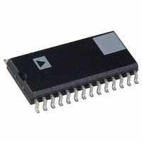
ADMCF326BRZ Analog Devices Inc, ADMCF326BRZ Datasheet - Page 9

ADMCF326BRZ
Manufacturer Part Number
ADMCF326BRZ
Description
IC DSP FLASH MOTOR CTRLR 28SOIC
Manufacturer
Analog Devices Inc
Series
Motor Controlr
Type
Fixed Pointr
Datasheet
1.ADMCF326BN.pdf
(36 pages)
Specifications of ADMCF326BRZ
Interface
Synchronous Serial Port (SSP)
Clock Rate
20MHz
Non-volatile Memory
FLASH (12 kB), ROM (12kB)
On-chip Ram
2.5kB
Voltage - I/o
5.00V
Voltage - Core
5.00V
Operating Temperature
-40°C ~ 85°C
Mounting Type
Surface Mount
Package / Case
28-SOIC (7.5mm Width)
Lead Free Status / RoHS Status
Lead free / RoHS Compliant
Available stocks
Company
Part Number
Manufacturer
Quantity
Price
Company:
Part Number:
ADMCF326BRZ
Manufacturer:
SHARP
Quantity:
1 000
Part Number:
ADMCF326BRZ
Manufacturer:
ADI/亚德诺
Quantity:
20 000
Serial Port
The ADMCF326 incorporates a complete synchronous serial port
(SPORT1) for serial communication and multiprocessor com-
munication. The following is a brief list of capabilities of the
ADMCF326 SPORT1. Refer to the ADSP-2100 Family User’s
Manual, Third Edition, for further details.
• SPORT1 is bidirectional and has a separate, double-buffered
• SPORT1 can use an external serial clock or generate its own
• SPORT1 has independent framing for the receive and trans-
• SPORT1 supports serial data-word lengths from three bits to 16
• SPORT1 receive and transmit sections can generate unique
• SPORT1 can receive and transmit an entire circular buffer of
• SPORT1 can be configured to have two external interrupts
• SPORT1 has two data receive pins (DR1A and DR1B), which
PIN FUNCTION DESCRIPTION
The ADMCF326 is available in both 28-lead SOIC and PDIP
packages. Table I describes the pins.
Pin Group
Name
RESET
SPORT1
CLKOUT
CLKIN, XTAL
PIO0–PIO8
AUX0–AUX1
AH–CL
PWMTRIP
V1, V2, V3
VAUX0–VAUX2 3
ICONST
V
GND
*
REV. B
Multiplexed pins, individually selectable through PIOSELECT and PIODATA1
Registers.
DD
transmit and receive section.
serial clock internally.
mit sections. Sections run in a frameless mode or with frame
synchronization signals internally or externally generated.
Frame synchronization signals are active high or inverted,
with either of two pulsewidths and timings.
bits and provides optional A-law and µ-law companding ac-
cording to ITU (formerly CCITT) recommendation G.711.
interrupts on completing a data-word transfer.
data with only one overhead cycle per data-word. An interrupt is
generated after a data buffer transfer.
(IRQ0 and IRQ1), and the Flag In and Flag Out signals.
The internally generated serial clock may still be used in
this configuration.
are internally multiplexed onto the one DR1 port of the
SPORT1. The particular data receive pin selected is deter-
mined by a bit in the MODECTRL register.
*
*
*
*
No.
of
Pins Output Function
1
6
1
2
9
2
6
1
3
1
1
1
Table I. Pin List
I
I/O
O
I, O
I/O
O
O
I
I
I
O
Input/
Processor Reset Input
Serial Port 1 Pins (TFS1, RFS1,
DT1, DR1A, DR1B, SCLK1)
Processor Clock Output
External Clock or Quartz
Crystal Connection Point
Digital I/O Port Pins
Auxiliary PWM Outputs
PWM Outputs
PWM Trip Signal
Analog Inputs
Auxiliary Analog Input
ADC Constant Current Source
Power Supply
Ground
–9–
INTERRUPT OVERVIEW
The ADMCF326 can respond to 16 different interrupt sources
with minimal overhead, five of which are internal DSP core
interrupts and 11 are from the motor control peripherals. The five
DSP core interrupts are SPORT1 receive (or IRQ0) and transmit
(or IRQ1), the internal timer, and two software interrupts. The
motor control peripheral interrupts are the nine programmable I/Os
and two from the PWM (PWMSYNC pulse and PWMTRIP).
All motor control interrupts are multiplexed into the DSP core
through the peripheral IRQ2 interrupt. The interrupts are internally
prioritized and individually maskable. A detailed description of the
entire interrupt system of the ADMCF326 is presented later,
following a more detailed description of each peripheral block.
MEMORY MAP
The ADMCF326 has two distinct memory types: program memory
and data memory. In general, program memory contains user
code and coefficients, while the data memory is used to store
variables and data during program execution. Three kinds of
program memory are provided on the ADMCF326: RAM, ROM,
and flash memory. The motor control peripherals are memory
mapped into a region of the data memory space starting at 0x2000.
The complete program and data memory maps are given in
Tables II and III, respectively.
Address Range
0x0000–0x002F
0x0030–0x01FF
0x0200–0x07FF
0x0800–0x17FF
0x1800–0x1FFF
0x2000–0x20FF
0x2100–0x21FF
0x2200–0x2FFF
0x3000–0x3FFF
Address Range
0x0000–0x1FFF
0x2000–0x20FF
0x2100–0x37FF
0x3800–0x39FF
0x3A00–0x3BFF
0x3C00–0x3FFF
Table II. Program Memory Map
Table III. Data Memory Map
Memory
Type
RAM
RAM
ROM
FLASH
FLASH
FLASH
Memory
Type
RAM
RAM
Function
Internal Vector Table
User Program Memory
Reserved
Reserved Program Memory
Reserved
User Program Memory
Sector 0
User Program Memory
Sector 1
User Program Memory
Sector 2
Reserved
Function
Reserved
Memory Mapped Registers
Reserved
User Data Memory
Reserved
Memory Mapped Registers
ADMCF326


