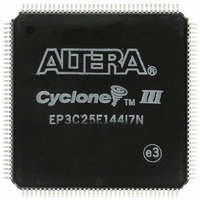
EP3C25E144I7N Altera, EP3C25E144I7N Datasheet - Page 32

EP3C25E144I7N
Manufacturer Part Number
EP3C25E144I7N
Description
IC CYCLONE III FPGA 25K 144 EQFP
Manufacturer
Altera
Series
Cyclone® IIIr
Datasheets
1.EP3C5F256C8N.pdf
(5 pages)
2.EP3C5F256C8N.pdf
(34 pages)
3.EP3C5F256C8N.pdf
(66 pages)
4.EP3C5F256C8N.pdf
(14 pages)
5.EP3C5F256C8N.pdf
(76 pages)
Specifications of EP3C25E144I7N
Number Of Logic Elements/cells
24624
Number Of Labs/clbs
1539
Total Ram Bits
608256
Number Of I /o
82
Voltage - Supply
1.15 V ~ 1.25 V
Mounting Type
Surface Mount
Operating Temperature
-40°C ~ 100°C
Package / Case
144-EQFP
For Use With
544-2601 - KIT DEV CYCLONE III LS EP3CLS200544-2411 - KIT DEV NIOS II CYCLONE III ED.544-2370 - KIT STARTER CYCLONE III EP3C25
Lead Free Status / RoHS Status
Lead free / RoHS Compliant
Number Of Gates
-
Other names
544-2542
Available stocks
Company
Part Number
Manufacturer
Quantity
Price
Company:
Part Number:
EP3C25E144I7N
Manufacturer:
IR
Quantity:
12 000
Company:
Part Number:
EP3C25E144I7N
Manufacturer:
ALTERA31
Quantity:
500
Page 32
f
Clocks
Clocks are important as they have a large effect on your design’s timing accuracy,
performance, and reliability. Problems associated with the clocks can cause functional
and timing problems in the design. Pay attention to the following sub-sections that are
related to clocks when you are in the designing stage.
Global Clock Pins and Clock Networks
Use dedicated clock pins and global clock routing for clock signal input to your
design. The dedicated clock pins drive the clock network directly, ensuring lower
skew compared to using normal I/O pins. High clock skew might cause hold time
violation. The clock network drives the entire Cyclone III device and you can use the
global clock to drive all the features in the device, for example the M9K memory and
logic array blocks. Using the clock network ensures you have a predictable and more
constant delay for signals that have high fan-out. You can also use the clock pins and
clock network to drive control signals such as asynchronous reset.
For more information about the global clock pins and clock networks, refer to the
Clock Networks and PLLs in Cyclone III Devices
Device Handbook.
Internally Generated Clocks
Combinational logic output is not immune to glitches as it depends on the inputs to
the circuit. The input signals may arrive at the combinational logic circuit at different
times and cause glitches. Moreover, the input signals may have glitches and the
combinational logic circuitry does not filter out these glitches. If you use this
combinational logic output signal as a clock to other circuitries, these glitches can
cause functional problems.
Always register the input signals to the combinational circuitry and the output signal
from that circuitry that is used as a clock
higher frequency than the clock generated internally. Registering the input signals to
the combinational circuitry ensures the arrival of the signals to the circuit is controlled
by the clock, and any glitches are filtered in the input signals. By registering the
output signals from the circuit, you can filter out any glitches generated by the
circuitry.
Figure 5. Registering the Input and Output Signals
Clock Signal of
Higher Frequency
Clock Signal of
Higher Frequency
Input
Signal
Input
Signal
Clock Generation
(Figure
Combinational
Circuitry
chapter in volume 1 of the Cyclone III
5) if you have a clock signal with a
© November 2008 Altera Corporation
Generated
Clock Signal
Design and Compilation


