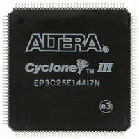
EP3C25E144I7N Altera, EP3C25E144I7N Datasheet - Page 62

EP3C25E144I7N
Manufacturer Part Number
EP3C25E144I7N
Description
IC CYCLONE III FPGA 25K 144 EQFP
Manufacturer
Altera
Series
Cyclone® IIIr
Datasheets
1.EP3C5F256C8N.pdf
(5 pages)
2.EP3C5F256C8N.pdf
(34 pages)
3.EP3C5F256C8N.pdf
(66 pages)
4.EP3C5F256C8N.pdf
(14 pages)
5.EP3C5F256C8N.pdf
(76 pages)
Specifications of EP3C25E144I7N
Number Of Logic Elements/cells
24624
Number Of Labs/clbs
1539
Total Ram Bits
608256
Number Of I /o
82
Voltage - Supply
1.15 V ~ 1.25 V
Mounting Type
Surface Mount
Operating Temperature
-40°C ~ 100°C
Package / Case
144-EQFP
For Use With
544-2601 - KIT DEV CYCLONE III LS EP3CLS200544-2411 - KIT DEV NIOS II CYCLONE III ED.544-2370 - KIT STARTER CYCLONE III EP3C25
Lead Free Status / RoHS Status
Lead free / RoHS Compliant
Number Of Gates
-
Other names
544-2542
Available stocks
Company
Part Number
Manufacturer
Quantity
Price
Company:
Part Number:
EP3C25E144I7N
Manufacturer:
IR
Quantity:
12 000
Company:
Part Number:
EP3C25E144I7N
Manufacturer:
ALTERA31
Quantity:
500
Page 62
“Board Design Considerations” on page 17
“Design and Compilation” on page 28
19
20
21
22
23
24
25
26
27
28
29
30
31
32
33
34
35
36
37
38
39
40
41
Done
Done
N/A
N/A
Use the correct hardware setup when interfacing the Cyclone III device with 3.3/3.0/2.5-V
LVTTL/LVCMOS I/O systems.
Use the Quartus II software to check the restriction on the pin placement.
Minimize the simultaneous switching noise effect on the board with the following methods:
l
l
l
l
l
Connect the device unused pins to the board according to the behavior of the pins.
Terminate the signals according to the I/O standard and signal travel direction.
Perform board-level IBIS or HSPICE simulation.
Minimize the noise on the power planes.
Consider the power-up requirement and I/O behavior of the Cyclone III device during power
up.
Add the correct series resistance to the appropriate configuration signals based on the
configuration scheme used.
Use repeater buffers for the configuration signals when cascading Cyclone III devices in
multi-device configuration.
Ensure that the
Pull the configuration pins high or low through resistors with the recommended values.
Ensure that the devices in a configuration chain are connected properly.
To prevent the signals to the configuration pins from overshooting to more than 4.1 V, use
series resistors and buffers according to the setup.
Do not leave the
Connect the
For AP configuration, select the flash memory from the Intel P30 and P33 families that can
support 40-MHz clock.
Check the pin connection for other pins of the configuration device or flash memory.
Use the
Depending on the on-chip debugging method used, reserve additional resources such as
LE, memory and I/O, and route the JTAG pins out.
Consider the trade-off between schematics or HDL for your design entry based on your
design’s complexity.
Other than the Quartus II software, consider building your design with third-party EDA tools,
SOPC Builder, or IP cores.
If you are using HDL for design entry, use the recommended coding styles.
Distributing simultaneous switching I/O to different I/O banks
Setting unused I/O pins to V
Turning on the slow slew rate feature for the switching pins
Using a lower drive strength for the switching pins
Using the proper termination scheme for the switching pins
areset
MSEL
DCLK
JTAG
,
locked
pins to V
or
pins unconnected.
TCK
CC A
or
signals are clean.
pfdena
C C
or ground directly based on the configuration scheme used.
or ground
control signals as required by your design.
© November 2008 Altera Corporation
Design Checklist


