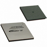
EP2SGX130GF1508I4N Altera, EP2SGX130GF1508I4N Datasheet - Page 290

EP2SGX130GF1508I4N
Manufacturer Part Number
EP2SGX130GF1508I4N
Description
IC STRATIX II GX 130K 1508-FBGA
Manufacturer
Altera
Series
Stratix® II GXr
Datasheet
1.EP2SGX30DF780C5.pdf
(316 pages)
Specifications of EP2SGX130GF1508I4N
Number Of Logic Elements/cells
132540
Number Of Labs/clbs
6627
Total Ram Bits
6747840
Number Of I /o
734
Voltage - Supply
1.15 V ~ 1.25 V
Mounting Type
Surface Mount
Operating Temperature
-40°C ~ 100°C
Package / Case
1508-FBGA
Family Name
Stratix II GX
Number Of Logic Blocks/elements
132540
# I/os (max)
734
Frequency (max)
732.1MHz
Process Technology
SRAM
Operating Supply Voltage (typ)
1.2V
Logic Cells
132540
Ram Bits
6747840
Operating Supply Voltage (min)
1.15V
Operating Supply Voltage (max)
1.25V
Operating Temp Range
-40C to 100C
Operating Temperature Classification
Industrial
Mounting
Surface Mount
Pin Count
1508
Package Type
FC-FBGA
Lead Free Status / RoHS Status
Lead free / RoHS Compliant
Number Of Gates
-
Lead Free Status / Rohs Status
Compliant
Other names
544-2175
Available stocks
Company
Part Number
Manufacturer
Quantity
Price
Company:
Part Number:
EP2SGX130GF1508I4N
Manufacturer:
Sunon
Quantity:
1 000
Part Number:
EP2SGX130GF1508I4N
Manufacturer:
ALTERA/阿尔特拉
Quantity:
20 000
- Current page: 290 of 316
- Download datasheet (2Mb)
Tables 4–98
derivation for different I/O standards on Stratix II GX devices. Examples
are also provided that show how to calculate DCD as a percentage.
Here is an example for calculating the DCD as a percentage for a
non-DDIO output on a row I/O on a -3 device:
If the non-DDIO output I/O standard is SSTL-2 Class II, the maximum
DCD is 95 ps (see
period T is:
To calculate the DCD as a percentage:
3.3-V LVTTTL
3.3-V LVCMOS
2.5 V
1.8 V
1.5-V LVCMOS
SSTL-2 Class I
SSTL-2 Class II
SSTL-18 Class I
1.8-V HSTL Class I
1.5-V HSTL Class I
LVDS
Row I/O Output Standard
Table 4–98. Maximum DCD for Non-DDIO Output on Row I/O Pins
T = 1/ f = 1 / 267 MHz = 3.745 ns = 3,745 ps
(T/2 – DCD) / T = (3,745 ps/2 – 95 ps) / 3,745 ps = 47.5% (for low
boundary)
(T/2 + DCD) / T = (3,745 ps/2 + 95 ps) / 3,745 ps = 52.5% (for high
boundary)
through
Table
4–105
4–99). If the clock frequency is 267 MHz, the clock
show the maximum DCD in absolution
-3 Devices
Maximum DCD (ps) for Non-DDIO Output
245
125
105
180
165
115
95
55
80
85
55
-4 and -5 Devices
275
155
135
180
195
145
125
100
115
85
80
Unit
ps
ps
ps
ps
ps
ps
ps
ps
ps
ps
ps
Related parts for EP2SGX130GF1508I4N
Image
Part Number
Description
Manufacturer
Datasheet
Request
R

Part Number:
Description:
CYCLONE II STARTER KIT EP2C20N
Manufacturer:
Altera
Datasheet:

Part Number:
Description:
CPLD, EP610 Family, ECMOS Process, 300 Gates, 16 Macro Cells, 16 Reg., 16 User I/Os, 5V Supply, 35 Speed Grade, 24DIP
Manufacturer:
Altera Corporation
Datasheet:

Part Number:
Description:
CPLD, EP610 Family, ECMOS Process, 300 Gates, 16 Macro Cells, 16 Reg., 16 User I/Os, 5V Supply, 15 Speed Grade, 24DIP
Manufacturer:
Altera Corporation
Datasheet:

Part Number:
Description:
Manufacturer:
Altera Corporation
Datasheet:

Part Number:
Description:
CPLD, EP610 Family, ECMOS Process, 300 Gates, 16 Macro Cells, 16 Reg., 16 User I/Os, 5V Supply, 30 Speed Grade, 24DIP
Manufacturer:
Altera Corporation
Datasheet:

Part Number:
Description:
High-performance, low-power erasable programmable logic devices with 8 macrocells, 10ns
Manufacturer:
Altera Corporation
Datasheet:

Part Number:
Description:
High-performance, low-power erasable programmable logic devices with 8 macrocells, 7ns
Manufacturer:
Altera Corporation
Datasheet:

Part Number:
Description:
Classic EPLD
Manufacturer:
Altera Corporation
Datasheet:

Part Number:
Description:
High-performance, low-power erasable programmable logic devices with 8 macrocells, 10ns
Manufacturer:
Altera Corporation
Datasheet:

Part Number:
Description:
Manufacturer:
Altera Corporation
Datasheet:

Part Number:
Description:
Manufacturer:
Altera Corporation
Datasheet:

Part Number:
Description:
Manufacturer:
Altera Corporation
Datasheet:

Part Number:
Description:
CPLD, EP610 Family, ECMOS Process, 300 Gates, 16 Macro Cells, 16 Reg., 16 User I/Os, 5V Supply, 25 Speed Grade, 24DIP
Manufacturer:
Altera Corporation
Datasheet:


