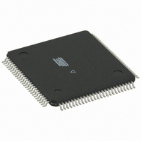
AT94K05AL-25AQU Atmel, AT94K05AL-25AQU Datasheet - Page 21

AT94K05AL-25AQU
Manufacturer Part Number
AT94K05AL-25AQU
Description
IC FPSLIC 5K GATE 25MHZ 100-TQFP
Manufacturer
Atmel
Series
FPSLIC®r
Datasheet
1.AT94K05AL-25AJI.pdf
(204 pages)
Specifications of AT94K05AL-25AQU
Core Type
8-bit AVR
Speed
25MHz
Interface
I²C, UART
Program Sram Bytes
4K-16K
Fpga Sram
2kb
Data Sram Bytes
4K ~ 16K
Fpga Core Cells
256
Fpga Gates
5K
Fpga Registers
436
Voltage - Supply
3 V ~ 3.6 V
Mounting Type
Surface Mount
Operating Temperature
-40°C ~ 85°C
Package / Case
100-TQFP, 100-VQFP
For Use With
ATSTK594 - BOARD FPSLIC DAUGHTER FOR STK500
Lead Free Status / RoHS Status
Lead free / RoHS Compliant
Eeprom Size
-
Available stocks
Company
Part Number
Manufacturer
Quantity
Price
- Current page: 21 of 204
- Download datasheet (4Mb)
3. FPGA/AVR Interface and System Control
3.1
1138I–FPSLI–1/08
FPGA/AVR Interface – Memory-mapped Peripherals
The FPGA and AVR share a flexible interface which allows for many methods of system
integration.
The FPGA core can be directly accessed by the AVR core, see
tions in the AVR memory map are decoded into 16 select lines (8 for AT94K05) and are
presented to the FPGA along with the AVR 8-bit data bus. The FPGA can be used to create
additional custom peripherals for the AVR microcontroller through this interface. In addition there
are 16 interrupt lines (8 for AT94K05) from the FPGA back into the AVR interrupt controller. Pro-
grammable peripherals or regular logic can use these interrupt lines. Full support for
programmable peripherals is available within the System Designer tool suite.
Figure 3-1.
The FPGA I/O selection is controlled by the AVR. This is described in detail beginning on
page
• Both FPGA and AVR share access to the 15 ns dual-port SRAM.
• The AVR data bus interfaces directly into the FPGA busing resources, effectively treating the
• Up to 16 decoded address lines are provided into the FPGA.
• Up to 16 interrupts are available from the FPGA to the AVR.
• The AVR can reprogram the FPGA during operation to create a dynamic reconfigurable
FPGA as a large I/O device. Users have complete flexibility on the types of additional
peripherals which are placed and routed inside the FPGA user logic.
system (Cache Logic).
FPGA CORE
EMBEDDED
55. The FPGA I/O interrupts are described beginning on
FPGA/AVR Interface: Interrupts and Addressing
Up to 16 Memory-mapped
Decoded Address
Lines from 4 I/O Memory
Space Addresses
Up to 16 Interrupt Lines from FPGA to AVR – Various Priority Levels
Data Out
Data In
8-bit
8-bit
ADDRESS
DECODER
DECODE
FPGAIOWE
8-bit Bi-directional Data Bus
4:16
AT94KAL Series FPSLIC
I/O Memory Address Bus
FPGAIORE
page
Figure
59.
3-1. Four memory loca-
EMBEDDED
AVR CORE
21
Related parts for AT94K05AL-25AQU
Image
Part Number
Description
Manufacturer
Datasheet
Request
R

Part Number:
Description:
IC FPSLIC 5K GATE 25MHZ 84PLCC
Manufacturer:
Atmel
Datasheet:

Part Number:
Description:
Fpslic Devices Combine 5K Gates of Atmel's Patented AT40K Fpga Architecture, a 20 Mips Avr 8-bit Risc Microprocessor Core, Numerous Fixed Microcontroller Peripheries And up to 36K Bytes of Program And Data SRAM.
Manufacturer:
ATMEL Corporation
Datasheet:

Part Number:
Description:
IC FPSLIC 5K GATE 25MHZ 84PLCC
Manufacturer:
Atmel
Datasheet:

Part Number:
Description:
IC FPSLIC 5K GATE 25MHZ 208PQFP
Manufacturer:
Atmel
Datasheet:

Part Number:
Description:
IC FPSLIC 5K GATE 25MHZ 144LQFP
Manufacturer:
Atmel
Datasheet:

Part Number:
Description:
IC FPSLIC 5K GATE 25MHZ 208PQFP
Manufacturer:
Atmel
Datasheet:

Part Number:
Description:
IC FPSLIC 5K GATE 25MHZ 144LQFP
Manufacturer:
Atmel
Datasheet:

Part Number:
Description:
IC FPSLIC 5K GATE 25MHZ 144-LQFP
Manufacturer:
Atmel
Datasheet:

Part Number:
Description:
Manufacturer:
Atmel
Datasheet:

Part Number:
Description:
Manufacturer:
Atmel
Datasheet:

Part Number:
Description:
Manufacturer:
Atmel
Datasheet:

Part Number:
Description:
5k - 40k Gates Of At40k Fpga With 8-bit Microcontroller, Up To 36k Bytes Of Sram And On-chip Jtag Ice
Manufacturer:
ATMEL Corporation
Datasheet:

Part Number:
Description:
At94k05al 5k - 40k Gates Of At40k Fpga With 8-bit Microcontroller, Up To 36k Bytes Of Sram And On-chip Jtag Ice
Manufacturer:
ATMEL Corporation
Datasheet:

Part Number:
Description:
DEV KIT FOR AVR/AVR32
Manufacturer:
Atmel
Datasheet:


