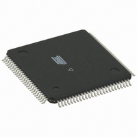
AT94K05AL-25AQU Atmel, AT94K05AL-25AQU Datasheet - Page 84

AT94K05AL-25AQU
Manufacturer Part Number
AT94K05AL-25AQU
Description
IC FPSLIC 5K GATE 25MHZ 100-TQFP
Manufacturer
Atmel
Series
FPSLIC®r
Datasheet
1.AT94K05AL-25AJI.pdf
(204 pages)
Specifications of AT94K05AL-25AQU
Core Type
8-bit AVR
Speed
25MHz
Interface
I²C, UART
Program Sram Bytes
4K-16K
Fpga Sram
2kb
Data Sram Bytes
4K ~ 16K
Fpga Core Cells
256
Fpga Gates
5K
Fpga Registers
436
Voltage - Supply
3 V ~ 3.6 V
Mounting Type
Surface Mount
Operating Temperature
-40°C ~ 85°C
Package / Case
100-TQFP, 100-VQFP
For Use With
ATSTK594 - BOARD FPSLIC DAUGHTER FOR STK500
Lead Free Status / RoHS Status
Lead free / RoHS Compliant
Eeprom Size
-
Available stocks
Company
Part Number
Manufacturer
Quantity
Price
- Current page: 84 of 204
- Download datasheet (4Mb)
4.22.3.3
4.22.3.4
84
AT94KAL Series FPSLIC
Scanning 2-wire Serial
Scanning the Clock Pins
The SCL and SDA pins are open drain, bi-directional and enabled separately. The “Enable Out-
put” bits (active High) in the scan chain are supported by general boundary-scan cells. Enabling
the output will drive the pin Low from a tri-state. External pull-ups on the 2-wire bus are required
to pull the pins High if the output is disabled. The “Data Out/In” and “Clock Out/In” bits in the
scan chain are observe-only cells.
chain.
Figure 4-23. Boundary-scan Cells for 2-wire Serial
Figure 4-24
The Enable signal is supported with a general boundary-scan cell, while the oscillator/clock out-
put is attached to an observe-only cell. In addition to the main clock, the timer oscillator is
scanned in the same way. The output from the internal RC-Oscillator is not scanned, as this
oscillator does not have external connections.
Figure 4-24. Boundary-scan Cells for Oscillators and Clock Options
From digital logic
shows how each oscillator with external connection is supported in the scan chain.
previous cell
To 2-wire
Serial Logic
From 2-wire
Serial Logic
From
ShiftDR
0
1
ClockDR UpdateDR
D Q
next
cell
To
Data or Clock Out/In
(Observe Only Cell)
D Q
G
From Previous Cell
To Next Cell
Enable Output
(General Boundary
Scan Cell)
Figure 4-23
EXTEST
0
1
XTAL1/TOSC1
ENABLE
shows how each pin is connected in the scan
Oscillator
XTAL2/TOSC2
OUTPUT
previous cell
From
ShiftDR
0
1
ClockDR
D Q
FF1
SDA or
SCL
next
cell
To
To system logic
1138I–FPSLI–1/08
Related parts for AT94K05AL-25AQU
Image
Part Number
Description
Manufacturer
Datasheet
Request
R

Part Number:
Description:
IC FPSLIC 5K GATE 25MHZ 84PLCC
Manufacturer:
Atmel
Datasheet:

Part Number:
Description:
Fpslic Devices Combine 5K Gates of Atmel's Patented AT40K Fpga Architecture, a 20 Mips Avr 8-bit Risc Microprocessor Core, Numerous Fixed Microcontroller Peripheries And up to 36K Bytes of Program And Data SRAM.
Manufacturer:
ATMEL Corporation
Datasheet:

Part Number:
Description:
IC FPSLIC 5K GATE 25MHZ 84PLCC
Manufacturer:
Atmel
Datasheet:

Part Number:
Description:
IC FPSLIC 5K GATE 25MHZ 208PQFP
Manufacturer:
Atmel
Datasheet:

Part Number:
Description:
IC FPSLIC 5K GATE 25MHZ 144LQFP
Manufacturer:
Atmel
Datasheet:

Part Number:
Description:
IC FPSLIC 5K GATE 25MHZ 208PQFP
Manufacturer:
Atmel
Datasheet:

Part Number:
Description:
IC FPSLIC 5K GATE 25MHZ 144LQFP
Manufacturer:
Atmel
Datasheet:

Part Number:
Description:
IC FPSLIC 5K GATE 25MHZ 144-LQFP
Manufacturer:
Atmel
Datasheet:

Part Number:
Description:
Manufacturer:
Atmel
Datasheet:

Part Number:
Description:
Manufacturer:
Atmel
Datasheet:

Part Number:
Description:
Manufacturer:
Atmel
Datasheet:

Part Number:
Description:
5k - 40k Gates Of At40k Fpga With 8-bit Microcontroller, Up To 36k Bytes Of Sram And On-chip Jtag Ice
Manufacturer:
ATMEL Corporation
Datasheet:

Part Number:
Description:
At94k05al 5k - 40k Gates Of At40k Fpga With 8-bit Microcontroller, Up To 36k Bytes Of Sram And On-chip Jtag Ice
Manufacturer:
ATMEL Corporation
Datasheet:

Part Number:
Description:
DEV KIT FOR AVR/AVR32
Manufacturer:
Atmel
Datasheet:


