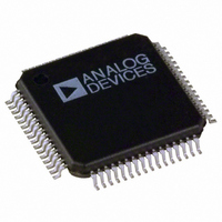
ADE7569ASTZF16 Analog Devices Inc, ADE7569ASTZF16 Datasheet - Page 115

ADE7569ASTZF16
Manufacturer Part Number
ADE7569ASTZF16
Description
IC ENERGY METER MCU 16K 64LQFP
Manufacturer
Analog Devices Inc
Specifications of ADE7569ASTZF16
Applications
Energy Measurement
Core Processor
8052
Program Memory Type
FLASH (16 kB)
Controller Series
ADE75xx
Ram Size
512 x 8
Interface
I²C, SPI, UART
Number Of I /o
20
Voltage - Supply
3.135 V ~ 3.465 V
Operating Temperature
-40°C ~ 85°C
Mounting Type
Surface Mount
Package / Case
64-LQFP
Ic Function
Single Phase Energy Measurement IC
Supply Voltage Range
3.13V To 3.46V, 2.4V To 3.7V
Operating Temperature Range
-40°C To +85°C
Digital Ic Case Style
LQFP
No. Of Pins
64
Lead Free Status / RoHS Status
Lead free / RoHS Compliant
Available stocks
Company
Part Number
Manufacturer
Quantity
Price
Company:
Part Number:
ADE7569ASTZF16
Manufacturer:
AD
Quantity:
310
Company:
Part Number:
ADE7569ASTZF16
Manufacturer:
Analog Devices Inc
Quantity:
10 000
Company:
Part Number:
ADE7569ASTZF16-RL
Manufacturer:
Analog Devices Inc
Quantity:
10 000
TIMERS
Each ADE7116/ADE7156/ADE7166/ADE7169/ADE7566/
ADE7569 has three 16-bit timer/counters: Timer/Counter 0,
Timer/Counter 1, and Timer/Counter 2. The timer/counter
hardware is included on-chip to relieve the processor core of
overhead inherent in implementing timer/counter functionality
in software. Each timer/counter consists of two 8-bit registers:
THx and TLx (x = 0, 1, or 2). All three timers can be configured
to operate as timers or as event counters.
When functioning as a timer, the TLx SFR is incremented every
machine cycle. (Users can think of it as counting machine cycles.)
Because a machine cycle on a single-cycle core consists of one core
clock period, the maximum count rate is the core clock frequency.
Table 112. Timer SFRs
SFR
TCON
TMOD
TL0
TL1
TH0
TH1
T2CON
RCAP2L
RCAP2H
TL2
TH2
TIMER REGISTERS
Table 113. Timer/Counter 0 and Timer/Counter 1 Mode SFR (TMOD, Address 0x89)
Bit
7
6
[5:4]
3
2
[1:0]
Mnemonic
Gate1
C/T1
T1/M1,
T1/M0
Gate0
C/T0
T0/M1,
T0/M0
Address
0x88
0x89
0x8A
0x8B
0x8C
0x8D
0xC8
0xCA
0xCB
0xCC
0xCD
Default
0
0
00
0
0
00
Description
Timer 1 gating control. Set by software to enable Timer/Counter 1 only when the INT1 pin is high and the
TR1 control is set. Cleared by software to enable Timer 1 whenever the TR1 control bit is set.
Timer 1 timer or counter select bit. Set by software to select counter operation (input from T1 pin). Cleared
by software to select the timer operation (input from internal system clock).
Timer 1 mode select bits.
T1/M1, T1/M0
00
01
10
11
Timer 0 gating control. Set by software to enable Timer/Counter 0 only when the INT0 pin is high and the TR0
control bit is set. Cleared by software to enable Timer 0 whenever the TR0 control bit is set in the
Timer/Counter 0 and Timer/Counter 1 control SFR (TCON, Address 0x88)
Timer 0 timer or counter select bit. Set by software to the select counter operation (input from T0 pin).
Cleared by software to the select timer operation (input from internal system clock).
Timer 0 mode select bits.
T0/M1, T0/M0
00
01
10
11
Bit Addressable
Yes
No
No
No
No
No
Yes
No
No
No
No
ADE7116/ADE7156/ADE7166/ADE7169/ADE7566/ADE7569
Result
TH1 (Address 0x8D) operates as an 8-bit timer/counter. TL1 (Address 0x8D) serves as
5-bit prescaler.
16-bit timer/counter. TH1 and TL1 are cascaded; there is no prescaler.
8-bit autoreload timer/counter. TH1 holds a value to reload into TL1 each time it overflows.
Timer/Counter 1 stopped.
Result
TH0 operates as an 8-bit timer/counter. TL0 serves as a 5-bit prescaler.
16-bit timer/counter. TH0 and TL0 are cascaded; there is no prescaler.
8-bit autoreload timer/counter. TH0 holds a value to reload into TL0 each time it overflows.
TL0 is an 8-bit timer/counter controlled by the standard Timer 0 control bits. TH0 is an
8-bit timer only, controlled by Timer 1 control bits.
Rev. B | Page 115 of 152
Description
Timer/Counter 0 and Timer/Counter 1 control (see Table 114).
Timer/Counter 0 and Timer./Counter 1 mode (see Table 113).
Timer 0 low byte (see Table 117).
Timer 1 low byte (see Table 119).
Timer 0 high byte (see Table 116).
Timer 1 high byte (see Table 118).
Timer/Counter 2 control (see Table 115).
Timer 2 reload/capture low byte (see Table 123).
Timer 2 reload/capture high byte (see Table 122).
Timer 2 low byte (Table 121).
Timer 2 high byte (see Table 120).
When functioning as a counter, the TLx register is incremented
by a 1-to-0 transition at its corresponding external input pin:
T0, T1, or T2. When the samples show a high in one cycle and a
low in the next cycle, the count is incremented. Because it takes
two machine cycles (two core clock periods) to recognize a 1-to-0
transition, the maximum count rate is half the core clock frequency.
There are no restrictions on the duty cycle of the external input
signal, but to ensure that a given level is sampled at least once
before it changes, it must be held for a minimum of one full
machine cycle. User configuration and control of all timer
operating modes is achieved via the SFRs listed in Table 112.


