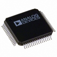
ADE7569ASTZF16 Analog Devices Inc, ADE7569ASTZF16 Datasheet - Page 75

ADE7569ASTZF16
Manufacturer Part Number
ADE7569ASTZF16
Description
IC ENERGY METER MCU 16K 64LQFP
Manufacturer
Analog Devices Inc
Specifications of ADE7569ASTZF16
Applications
Energy Measurement
Core Processor
8052
Program Memory Type
FLASH (16 kB)
Controller Series
ADE75xx
Ram Size
512 x 8
Interface
I²C, SPI, UART
Number Of I /o
20
Voltage - Supply
3.135 V ~ 3.465 V
Operating Temperature
-40°C ~ 85°C
Mounting Type
Surface Mount
Package / Case
64-LQFP
Ic Function
Single Phase Energy Measurement IC
Supply Voltage Range
3.13V To 3.46V, 2.4V To 3.7V
Operating Temperature Range
-40°C To +85°C
Digital Ic Case Style
LQFP
No. Of Pins
64
Lead Free Status / RoHS Status
Lead free / RoHS Compliant
Available stocks
Company
Part Number
Manufacturer
Quantity
Price
Company:
Part Number:
ADE7569ASTZF16
Manufacturer:
AD
Quantity:
310
Company:
Part Number:
ADE7569ASTZF16
Manufacturer:
Analog Devices Inc
Quantity:
10 000
Company:
Part Number:
ADE7569ASTZF16-RL
Manufacturer:
Analog Devices Inc
Quantity:
10 000
ENERGY-TO-FREQUENCY CONVERSION
The ADE7116/ADE7156/ADE7166/ADE7169/ADE7566/
ADE7569 also provide two energy-to-frequency conversions for
calibration purposes. After initial calibration at manufacturing,
the manufacturer or end customer often verifies the energy meter
calibration. One convenient way to do this is for the manufacturer
to provide an output frequency that is proportional to the active
power, reactive power, apparent power, or I
conditions. This output frequency can provide a simple single-
wire, optically isolated interface to external calibration equipment.
Figure 79 illustrates the energy-to-frequency conversion in the
ADE7116/ADE7156/ADE7166/ ADE7169/ADE7566/ADE7569.
Two digital-to-frequency converters (DFC) are used to generate
the pulsed outputs. When WDIV = 0 or 1, the DFC generates a
pulse each time 1 LSB in the energy register is accumulated. An
output pulse is generated when a CFxNUM/CFxDEN number
of pulses is generated at the DFC output. Under steady load
conditions, the output frequency is proportional to the active
power, reactive power, apparent power, or I
CFxSEL bits in the MODE2 register (Address 0x0C).
Both pulse outputs can be enabled or disabled by clearing or
setting the DISCF1 bit (Bit 1) and the DISCF2 bit (Bit 2) in the
MODE1 register (Address 0x0B), respectively.
Both pulse outputs set separate flags in the Interrupt Status 2 SFR
(MIRQSTM, Address 0xDD): CF1 (Bit 6) and CF2 (Bit 7). If the
CF1 enable bit (Bit 6) and CF2 enable bit (Bit 7) in the Interrupt
I
VA
* AVAILABLE ONLY IN THE ADE7569 AND ADE7169
rms
VARMSCFCON
MODE2 REGISTER 0x0C
VAR *
WATT
VOLTAGE CHANNEL
Figure 79. Energy-to-Frequency Conversion
CFxSEL[1:0]
FROM
ADC
DFC
LPF1
APPARENT POWER
CFxNUM
CFxDEN
÷
rms
ZERO-CROSSING
rms
DETECTION
under steady load
, depending on the
ADE7116/ADE7156/ADE7166/ADE7169/ADE7566/ADE7569
Figure 78. Line Cycle Apparent Energy Accumulation
or I
rms
CFx PULSE
OUTPUT
VADIV[7:0]
%
LINCYC[15:0]
Rev. B | Page 75 of 152
CALIBR ATION
CONTROL
+
+
Enable 2 SFR (MIRQENM, Address 0xDA) are set, the 8052 core
has a pending ADE interrupt. The ADE interrupt stays active
until the CF1 or CF2 status bit is cleared (see the Energy
Measurement Interrupts section).
Pulse Output Configuration
The two pulse output circuits have separate configuration bits
in the MODE2 register (Address 0x0C). Setting the CFxSEL bits
to 0b00, 0b01, or 0b1X configures the DFC to create a pulse
output proportional to active power , reactive power (ADE7169/
ADE7569 only), or apparent power or I
The selection between I
VARMSCFCON bit in the MODE2 register (Address 0x0C).
With this selection, CF2 cannot be proportional to apparent
power if CF1 is proportional to I
proportional to apparent power if CF2 is proportional to I
Pulse Output Characteristic
The pulse output for both DFCs stays low for 90 ms if the pulse
period is longer than 180 ms (5.56 Hz). If the pulse period is
shorter than 180 ms, the duty cycle of the pulse output is 50%.
The pulse output is active low and should be connected to an
LED, as shown in Figure 80.
The maximum output frequency with ac input signals at
full scale and with CFxNUM = 0x00 and CFxDEN = 0x00
is approximately 21.1 kHz.
The ADE7116/ADE7156/ADE7166/ADE7169/ADE7566/
ADE7569 incorporate two registers per DFC, CFxNUM[15:0]
and CFxDEN[15:0], to set the CFx frequency. These unsigned,
16-bit registers can be used to adjust the CFx frequency to a wide
range of values. These frequency scaling registers are 16-bit
registers that can scale the output frequency by 1/2
a step of 1/2
48
23
LVAHR[23:0]
16
.
Figure 80. CF Pulse Output
0
rms
CF
and apparent power is done by the
LVAHR REGISTER IS
UPDATED EVERY LINCYC
ZERO CROSSING WITH THE
TOTAL APPARENT ENERGY
DURING THAT DURATION
V
rms
DD
, and CF1 cannot be
0
rms
, respectively.
16
to 1 with
rms
.


