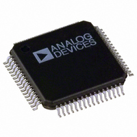
ADE7569ASTZF16 Analog Devices Inc, ADE7569ASTZF16 Datasheet - Page 19

ADE7569ASTZF16
Manufacturer Part Number
ADE7569ASTZF16
Description
IC ENERGY METER MCU 16K 64LQFP
Manufacturer
Analog Devices Inc
Specifications of ADE7569ASTZF16
Applications
Energy Measurement
Core Processor
8052
Program Memory Type
FLASH (16 kB)
Controller Series
ADE75xx
Ram Size
512 x 8
Interface
I²C, SPI, UART
Number Of I /o
20
Voltage - Supply
3.135 V ~ 3.465 V
Operating Temperature
-40°C ~ 85°C
Mounting Type
Surface Mount
Package / Case
64-LQFP
Ic Function
Single Phase Energy Measurement IC
Supply Voltage Range
3.13V To 3.46V, 2.4V To 3.7V
Operating Temperature Range
-40°C To +85°C
Digital Ic Case Style
LQFP
No. Of Pins
64
Lead Free Status / RoHS Status
Lead free / RoHS Compliant
Available stocks
Company
Part Number
Manufacturer
Quantity
Price
Company:
Part Number:
ADE7569ASTZF16
Manufacturer:
AD
Quantity:
310
Company:
Part Number:
ADE7569ASTZF16
Manufacturer:
Analog Devices Inc
Quantity:
10 000
Company:
Part Number:
ADE7569ASTZF16-RL
Manufacturer:
Analog Devices Inc
Quantity:
10 000
Table 14. Pin Function Descriptions
Pin No.
1
2
3
4
5
6
7
8
9
10
11
12
13
14
15
16
17
Mnemonic
COM3/FP27
COM2/FP28
COM1
COM0
P1.2/FP25
P1.3/T2EX/FP24
P1.4/T2/FP23
P1.5/FP22
P1.6/FP21
P1.7/FP20
P0.1/FP19
P2.0/FP18
P2.1/FP17
P2.2/FP16
LCDVC
LCDVP2
LCDVB
Common Output 1. COM1 is used for the LCD backplane.
Common Output 0. COM0 is used for the LCD backplane.
General-Purpose Digital I/O Port 1.2/LCD Segment Output 25.
General-Purpose Digital I/O Port 1.3/Timer 2 Control Input/LCD Segment Output 24.
General-Purpose Digital I/O Port 1.4/Timer 2 Input/LCD Segment Output 23.
General-Purpose Digital I/O Port 1.5/LCD Segment Output 22.
General-Purpose Digital I/O Port 1.6/LCD Segment Output 21.
General-Purpose Digital I/O Port 1.7/LCD Segment Output 20.
General-Purpose Digital I/O Port 0.1/LCD Segment Output 19.
General-Purpose Digital I/O Port 2.0/LCD Segment Output 18.
General-Purpose Digital I/O Port 2.1/LCD Segment Output 17.
General-Purpose Digital I/O Port 2.2/LCD Segment Output 16.
Description
Common Output 3/LCD Segment Output 27. COM3 is used for the LCD backplane.
Common Output 2/LCD Segment Output 28. COM2 is used for the LCD backplane.
In the ADE7166/ADE7169, this pin can be either an analog input when the LCD resistor driver is enabled or
an analog output when the LCD charge pump is enabled. In the ADE7116/ADE7156, this pin is always an
analog input. When this pin is an analog output, it should be decoupled with a 470 nF capacitor. When this
pin is an analog input, it is internally connected to V
LCDVB to generate the two highest voltages for the LCD waveforms (see the LCD Driver section).
In the ADE7166/ADE7169, this pin can be either an analog input when the LCD resistor driver is enabled or
an analog output when the LCD charge pump is enabled. In the ADE7116 and ADE7156, this pin is always an
analog input. When this pin is an analog output, a 100 nF capacitor should be connected between this pin and
LCDVP1. When this pin is an analog input, it is internally connected to LCDVP1 (see the LCD Driver section).
In the ADE7166/ADE7169, this pin can be either an analog input when the LCD resistor driver is enabled or
an analog output when the LCD charge pump is enabled. In the ADE7116/ADE7156, this pin is always an
analog input. When this pin is an analog output, it should be decoupled with a 470 nF capacitor. When this
pin is an analog input, a resistor should be connected between this pin and LCDVC to generate an
intermediate voltage for the LCD driver. In 1/3 bias LCD mode, another resistor must be connected between
this pin and LCDVA to generate another intermediate voltage. In 1/2 bias LCD mode, LCDVB and LCDVA are
internally connected (see the LCD Driver section).
P1.3/T2EX/FP24
NOTES
1. IT IS RECOMMENDED THAT THE EXPOSED PAD ON THE BOTTOM OF THE LFCSP BE
CONNECTED TO THE GROUND PLANE ON THE BOARD.
P1.4/T2/FP23
COM3/FP27
COM2/FP28
P1.2/FP25
P1.5/FP22
P1.6/FP21
P1.7/FP20
P0.1/FP19
P2.0/FP18
P2.1/FP17
P2.2/FP16
LCDVP2
Figure 10. Pin Configuration for the ADE7116/ADE7156/ADE7166/ADE7169
LCDVC
COM1
COM0
10
11
12
13
14
15
16
1
2
3
4
5
6
7
8
9
ADE7116/ADE7156/ADE7166/
PIN 1
INDICATOR
ADE7116/ADE7156/
ADE7166/ADE7169
Rev. B | Page 19 of 152
(Not to Scale)
TOP VIEW
DD
. A resistor should be connected between this pin and
48
47
46
45
44
43
42
41
40
39
38
37
36
35
34
33
INT0
XTAL1
XTAL2
BCTRL/INT1/P0.0
SDEN/P2.3
P0.2/CF1/RTCCAL
P0.3/CF2
P0.4/MOSI/SDATA
P0.5/MISO
P0.6/SCLK/T0
P0.7/SS/T1
P1.0/RxD
P1.1/TxD
FP0
FP1
FP2
ADE7169/ADE7566/ADE7569


