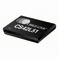
CS42L51-CNZ Cirrus Logic Inc, CS42L51-CNZ Datasheet - Page 38

CS42L51-CNZ
Manufacturer Part Number
CS42L51-CNZ
Description
IC CODEC STEREO W/HDPN AMP 32QFN
Manufacturer
Cirrus Logic Inc
Type
Stereo Audior
Datasheet
1.CS42L51-CNZ.pdf
(88 pages)
Specifications of CS42L51-CNZ
Package / Case
32-QFP
Data Interface
PCM Audio Interface
Resolution (bits)
24 b
Number Of Adcs / Dacs
2 / 2
Sigma Delta
Yes
Dynamic Range, Adcs / Dacs (db) Typ
98 / 98
Voltage - Supply, Analog
1.8V, 2.5V
Voltage - Supply, Digital
1.8V, 2.5V
Operating Temperature
-10°C ~ 70°C
Mounting Type
Surface Mount
Number Of Adc Inputs
6
Number Of Dac Outputs
2
Conversion Rate
96 KSPS
Interface Type
Serial (2-Wire, 3-Wire, I2C, SPI)
Resolution
24 bit
Operating Supply Voltage
1.8 V / 2.5 V
Maximum Operating Temperature
+ 70 C
Mounting Style
SMD/SMT
Minimum Operating Temperature
- 10 C
Number Of Channels
2 ADC/2 DAC
Thd Plus Noise
- 88 dB ADC / - 86 dB DAC
Peak Reflow Compatible (260 C)
No
Leaded Process Compatible
No
Rohs Compliant
Yes
Lead Free Status / RoHS Status
Lead free / RoHS Compliant
For Use With
598-1005 - BOARD EVAL FOR CS42L51 CODEC
Lead Free Status / Rohs Status
Lead free / RoHS Compliant
Other names
598-1045
Available stocks
Company
Part Number
Manufacturer
Quantity
Price
Company:
Part Number:
CS42L51-CNZ
Manufacturer:
CIRRUS
Quantity:
160
Company:
Part Number:
CS42L51-CNZ
Manufacturer:
CIRRUS
Quantity:
162
Part Number:
CS42L51-CNZ
Manufacturer:
CIRRUS
Quantity:
20 000
Company:
Part Number:
CS42L51-CNZR
Manufacturer:
Cirrus Logic Inc
Quantity:
10 000
38
4.4.8
4.5
Serial Port Clocking
The CODEC serial audio interface port operates either as a slave or master. It accepts externally generated
clocks in slave mode and will generate synchronous clocks derived from an input master clock (MCLK) in
master mode.
The frequency of the MCLK must be an integer multiple of, and synchronous with, the system sample rate,
Fs. The LRCK frequency is equal to Fs, the frequency at which audio samples for each channel are clocked
into or out of the device.
The SPEED and MCLKDIV2 software control bits or the SDOUT/(M/S) and MCLKDIV2 stand-alone control
pins, configure the device to generate the proper clocks in Master Mode and receive the proper clocks in
Slave Mode. The value on the SDOUT pin is latched immediately after powering up in Hardware Mode.
On-Chip Charge Pump
An on-chip charge pump derives a negative supply voltage from the VA_HP supply. This provides dual
rail supplies allowing a full-scale output swing centered around ground and eliminates the need for large,
DC-blocking capacitors. Added benefits include greater pop suppression and improved low frequency
(bass) response. Note: Series resistance in the path of the power supplies must be avoided. Any voltage
drop on the VA_HP supply will directly impact the derived negative voltage on the charge pump supply,
VSS_HP, and may result in clipping.
The FLYN and FLYP pins connect to internal switches that charges and discharges the external capacitor
attached, at a default switching frequency. This frequency may be adjusted in the control port registers.
Increasing the charge-pumping capacitor will slightly decease the pumping frequency. The capacitor con-
nected to VSS_HP acts as a charge reservoir for the negative supply as well as a filter for the ripple in-
duced by the charge pump. Increasing this capacitor will decrease the ripple on VSS_HP. Refer to the
typical connection diagrams in
values for the charge pump circuitry.
Software
Controls:
Hardware
Software
Control:
Control:
“MIC Power Control & Speed Control (Address 03h)” on page
(Address 09h)” on page
“Charge Pump Frequency (Address 21h)” on page
“SDOUT, M/S” pin 29
“MCLKDIV2” pin 2
Figure 1 on page 10
Pin
58.
or
Figure 2 on page 11
47 kΩ Pull-down
47 kΩ Pull-up
Setting
LO
HI
74.
for the recommended capacitor
Slave
Master
No Divide
MCLK is divided by 2 prior
to all internal circuitry.
50,
“DAC Control
Selection
CS42L51
DS679F1


