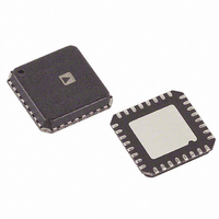
ADAU1361BCPZ Analog Devices Inc, ADAU1361BCPZ Datasheet - Page 24

ADAU1361BCPZ
Manufacturer Part Number
ADAU1361BCPZ
Description
IC CODEC 24B PLL 32LFCSP
Manufacturer
Analog Devices Inc
Type
Audio Codecr
Datasheet
1.ADAU1361BCPZ-RL.pdf
(80 pages)
Specifications of ADAU1361BCPZ
Data Interface
Serial
Resolution (bits)
24 b
Number Of Adcs / Dacs
2 / 2
Sigma Delta
No
Voltage - Supply, Analog
1.8 V ~ 3.6 V
Voltage - Supply, Digital
1.8 V ~ 3.6 V
Operating Temperature
-40°C ~ 85°C
Mounting Type
Surface Mount
Package / Case
32-VFQFN, CSP Exposed Pad
Audio Codec Type
Stereo
No. Of Adcs
2
No. Of Dacs
2
No. Of Input Channels
6
No. Of Output Channels
7
Adc / Dac Resolution
24bit
Adcs / Dacs Signal To Noise Ratio
101dB
Lead Free Status / RoHS Status
Lead free / RoHS Compliant
Available stocks
Company
Part Number
Manufacturer
Quantity
Price
Company:
Part Number:
ADAU1361BCPZ
Manufacturer:
TOSHIBA
Quantity:
1 650
Company:
Part Number:
ADAU1361BCPZ
Manufacturer:
ADI
Quantity:
624
Part Number:
ADAU1361BCPZ
Manufacturer:
ADI/亚德诺
Quantity:
20 000
Part Number:
ADAU1361BCPZ-R7
Manufacturer:
ADI/亚德诺
Quantity:
20 000
ADAU1361
STARTUP, INITIALIZATION, AND POWER
This section describes the procedure for properly starting up
the ADAU1361. The following sequence provides a high level
approach to the proper initiation of the system.
1.
2.
3.
4.
POWER-UP SEQUENCE
The ADAU1361 uses a power-on reset (POR) circuit to
reset the registers upon power-up. The POR monitors the
DVDDOUT pin and generates a reset signal whenever power
is applied to the chip. During the reset, the ADAU1361 is set
to the default values documented in the register map (see the
Control Registers section). Typically, with a 10 μF capacitor on
AVDD, the POR takes approximately 14 ms.
The PLL lock time is dependent on the MCLK rate. Typical
lock times are provided in Table 11.
Table 11. PLL Lock Times
PLL Mode
Fractional
Fractional
Integer
Fractional
Fractional
Fractional
Fractional
Fractional
Fractional
Integer
Fractional
Fractional
DVDDOUT
AVDD
POR
Apply power to the ADAU1361.
Lock the PLL to the input clock (if using the PLL).
Enable the core clock.
Load the register settings.
ACTIVE
POR
Figure 28. Power-On Reset Sequence
POR
FINISHED
MCLK Frequency
8 MHz
12 MHz
12.288 MHz
13 MHz
14.4 MHz
19.2 MHz
19.68 MHz
19.8 MHz
24 MHz
24.576 MHz
26 MHz
27 MHz
1.35V
PART READY
1.5V
Lock Time (Typical)
3.5 ms
3.0 ms
2.96 ms
2.4 ms
2.4 ms
2.98 ms
2.98 ms
2.98 ms
2.95 ms
2.96 ms
2.4 ms
2.4 ms
0.95V
POR ACTIVE
Rev. C | Page 24 of 80
POWER REDUCTION MODES
Sections of the ADAU1361 chip can be turned on and off as
needed to reduce power consumption. These include the ADCs,
the DACs, and the PLL.
In addition, the control registers can be used to configure some
functions for power saving, normal, or enhanced performance
operation. See the Control Registers section for more
information.
The digital filters of the ADCs and DACs can each be set to over-
sampling ratios of 64× or 128× (default). Setting the oversampling
ratios to 64× for these filters lowers power consumption with a
minimal impact on performance. See the Digital Filters section
for specifications; see the Typical Performance Characteristics
section for graphs of these filters.
DIGITAL POWER SUPPLY
The digital power supply for the ADAU1361 is generated from
an internal regulator. This regulator generates a 1.5 V supply
internally. The only external connection to this regulator is the
DVDDOUT bypassing point. A 100 nF capacitor and a 10 μF
capacitor should be connected between this pin and DGND.
INPUT/OUTPUT POWER SUPPLY
The power for the digital output pins is supplied from IOVDD,
and this pin also sets the highest input voltage that should be
seen on the digital input pins. IOVDD should be set between
1.8 V and 3.3 V; no digital input signal should be at a voltage
level higher than the one on IOVDD. The current draw of this
pin is variable because it depends on the loads of the digital
outputs. IOVDD should be decoupled to DGND with a 100 nF
capacitor and a 10 μF capacitor.
CLOCK GENERATION AND MANAGEMENT
The ADAU1361 uses a flexible clocking scheme that enables the
use of many different input clock rates. The PLL can be bypassed
or used, resulting in two different approaches to clock manage-
ment. For more information about clocking schemes, PLL
configuration, and sampling rates, see the Clocking and
Sampling Rates section.
Case 1: PLL Is Bypassed
If the PLL is bypassed, the core clock is derived directly from
the MCLK input. The rate of this clock must be set properly in
Register R0 (clock control register, Address 0x4000) using the
INFREQ[1:0] bits. When the PLL is bypassed, supported external
clock rates are 256 × f
is the base sampling rate. The core clock of the chip is off until
the core clock enable bit (COREN) is asserted.
S
, 512 × f
S
, 768 × f
S
, and 1024 × f
S
, where f
S


