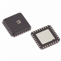
ADAU1361BCPZ Analog Devices Inc, ADAU1361BCPZ Datasheet - Page 39

ADAU1361BCPZ
Manufacturer Part Number
ADAU1361BCPZ
Description
IC CODEC 24B PLL 32LFCSP
Manufacturer
Analog Devices Inc
Type
Audio Codecr
Datasheet
1.ADAU1361BCPZ-RL.pdf
(80 pages)
Specifications of ADAU1361BCPZ
Data Interface
Serial
Resolution (bits)
24 b
Number Of Adcs / Dacs
2 / 2
Sigma Delta
No
Voltage - Supply, Analog
1.8 V ~ 3.6 V
Voltage - Supply, Digital
1.8 V ~ 3.6 V
Operating Temperature
-40°C ~ 85°C
Mounting Type
Surface Mount
Package / Case
32-VFQFN, CSP Exposed Pad
Audio Codec Type
Stereo
No. Of Adcs
2
No. Of Dacs
2
No. Of Input Channels
6
No. Of Output Channels
7
Adc / Dac Resolution
24bit
Adcs / Dacs Signal To Noise Ratio
101dB
Lead Free Status / RoHS Status
Lead free / RoHS Compliant
Available stocks
Company
Part Number
Manufacturer
Quantity
Price
Company:
Part Number:
ADAU1361BCPZ
Manufacturer:
TOSHIBA
Quantity:
1 650
Company:
Part Number:
ADAU1361BCPZ
Manufacturer:
ADI
Quantity:
624
Part Number:
ADAU1361BCPZ
Manufacturer:
ADI/亚德诺
Quantity:
20 000
Part Number:
ADAU1361BCPZ-R7
Manufacturer:
ADI/亚德诺
Quantity:
20 000
The R/ W bit determines the direction of the data. A Logic 0 on
the LSB of the first byte means that the master will write infor-
mation to the peripheral, whereas a Logic 1 means that the
master will read information from the peripheral after writing
the subaddress and repeating the start address. A data transfer
takes place until a stop condition is encountered. A stop
condition occurs when SDA transitions from low to high while
SCL is held high.
and
Stop and start conditions can be detected at any stage during the
data transfer. If these conditions are asserted out of sequence with
normal read and write operations, the ADAU1361 immediately
jumps to the idle condition. During a given SCL high period,
the user should only issue one start condition, one stop condition,
(CONTINUED)
(CONTINUED)
Figure 49
(CONTINUED)
(CONTINUED)
(CONTINUED)
(CONTINUED)
START BY
MASTER
SDA
SCL
START BY
MASTER
SDA
SCL
SDA
SDA
SDA
SCL
SCL
SCL
shows an I
Figure 48
0
0
2
C read.
1
shows the timing of an I
1
1
SUBADDRESS BYTE 2
CHIP ADDRESS BYTE
READ DATA BYTE 1
1
CHIP ADDRESS BYTE
1
SUBADDRESS BYTE 2
FRAME 1
FRAME 3
FRAME 5
1
FRAME 1
0
FRAME 3
ADDR1
0
ADDR1
Figure 49. I
ADDR0
Figure 48. I
2
C write,
ADDR0
R/W
ADAU1361
2
C Read from ADAU1361 Clocking
Rev. C | Page 39 of 80
2
ADAU1361
MASTER
R/W
C Write to ADAU1361 Clocking
ACK BY
ACK BY
ACK BY
ADAU1361
ADAU1361
ACK BY
ACK BY
STOP BY
MASTER
or a single stop condition followed by a single start condition. If
an invalid subaddress is issued by the user, the ADAU1361 does
not issue an acknowledge and returns to the idle condition.
If the user exceeds the highest subaddress while in autoincrement
mode, one of two actions is taken. In read mode, the ADAU1361
outputs the highest subaddress register contents until the master
device issues a no acknowledge, indicating the end of a read. A
no acknowledge condition is where the SDA line is not pulled
low on the ninth clock pulse on SCL. If the highest subaddress
location is reached while in write mode, the data for the invalid
byte is not loaded into any subaddress register, a no acknowledge
is issued by the ADAU1361, and the part returns to the idle
condition.
REPEATED
START BY MASTER
0
SUBADDRESS BYTE 1
1
SUBADDRESS BYTE 1
FRAME 2
CHIP ADDRESS BYTE
DATA BYTE 1
FRAME 4
1
FRAME 2
FRAME 4
1
0
ADDR1
ADAU1361
ADDR0
ACK BY
ADAU1361
ADAU1361
ACK BY
ACK BY
R/W
ADAU1361
ADAU1361
ACK BY
STOP BY
MASTER


