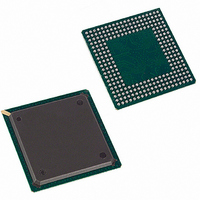
DS3112 Maxim Integrated Products, DS3112 Datasheet - Page 71

DS3112
Manufacturer Part Number
DS3112
Description
IC MUX TEMPE T3/E3 256-BGA
Manufacturer
Maxim Integrated Products
Datasheet
1.DS3112.pdf
(133 pages)
Specifications of DS3112
Controller Type
Framer, Multiplexer
Interface
Parallel/Serial
Voltage - Supply
3.135 V ~ 3.465 V
Current - Supply
150mA
Operating Temperature
0°C ~ 70°C
Mounting Type
Surface Mount
Package / Case
256-PBGA
Lead Free Status / RoHS Status
Contains lead / RoHS non-compliant
Available stocks
Company
Part Number
Manufacturer
Quantity
Price
Company:
Part Number:
DS3112+
Manufacturer:
Maxim Integrated Products
Quantity:
135
Company:
Part Number:
DS3112+
Manufacturer:
VISHAY
Quantity:
23 212
Part Number:
DS3112+
Manufacturer:
DALLAS
Quantity:
20 000
Part Number:
DS3112D1
Manufacturer:
DALLAS
Quantity:
20 000
Part Number:
DS3112N+
Manufacturer:
DALLAS
Quantity:
20 000
7.5 T1/E1 Loopback Control Register Description
Register Name:
Register Description:
Register Address:
Bit #
Name
Default
Bit #
Name
Default
Note: Bits that are underlined are read-only; all other bits are read-write.
Bits 0 to 15: T1/E1 Line Loopback Enable for Ports 1 to 16 (LLB1 to LLB16). These bits enable or disable the
T1/E1 Line Loopback (LLB). See the Block Diagrams in Section
corresponds to T1/E1 Port 1, LLB2 corresponds to T1/E1 Port 2, and so on. Since ports 4, 8, 12, 16, 20, 24, and 28
are not active in the G.747 mode, the LLB4, LLB8, LLB12, and LLB16 bits have no effect in the G.747 mode.
Register Name:
Register Description:
Register Address:
Bit #
Name
Default
Bit #
Name
Default
Note: Bits that are underlined are read-only; all other bits are read-write.
Bits 0 to 11: T1 Line Loopback Enable for Ports 17 to 28 (LLB17 to LLB28). These bits enable or disable the
T1 Line Loopback (LLB). See the block diagrams in Section
corresponds to T17 Port 17, LLB18 corresponds to T1 Port 18, and so on. Since ports 17 to 28 are not active in the
E3 mode, these bits have no effect in the E3 mode. Since ports 4, 8, 12, 16, 20, 24, and 28 are not active in the
G.747 mode, the LLB20, LLB24, and LLB28 bits have no effect in the G.747 mode.
0 = disable loopback
1 = enable loopback
0 = disable loopback
1 = enable loopback
LLB16
LLB24
LLB8
15
15
—
—
7
0
0
7
0
LLB15
LLB23
LLB7
14
14
—
—
6
0
0
6
0
T1E1LLB1
T1/E1 Line Loopback Control Register 1
50h
T1E1LLB2
T1/E1 Line Loopback Control Register 2
52h
LLB14
LLB22
LLB6
13
13
—
—
5
5
0
0
0
LLB13
LLB21
71 of 133
LLB5
12
12
—
—
4
0
0
4
0
1
LLB12
1
LLB20
LLB28
for a visual description of this loopback. LLB1
LLB4
for a visual description of this loopback. LLB1
11
11
3
3
0
0
0
0
LLB11
LLB19
LLB27
LLB3
10
10
2
0
0
2
0
0
LLB10
LLB18
LLB26
LLB2
1
9
1
9
0
0
0
0
LLB17
LLB25
LLB1
LLB9
DS3112
0
0
8
0
0
0
8
0


