DS26521LN+ Maxim Integrated Products, DS26521LN+ Datasheet - Page 23
DS26521LN+
Manufacturer Part Number
DS26521LN+
Description
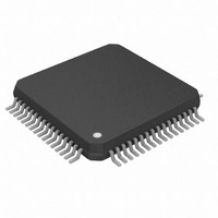
IC TXRX T1/E1/J1 64-LQFP
Manufacturer
Maxim Integrated Products
Type
Line Interface Units (LIUs)r
Datasheet
1.DS26521LN.pdf
(258 pages)
Specifications of DS26521LN+
Number Of Drivers/receivers
1/1
Protocol
T1/E1/J1
Voltage - Supply
3.135 V ~ 3.465 V
Mounting Type
Surface Mount
Package / Case
64-LQFP
Lead Free Status / RoHS Status
Lead free / RoHS Compliant


REFCLKIO
SPI_SCLK
SPI_MOSI
SPI_MISO
SPI_SEL
RESETB
NAME
MCLK
WRB /
RDB /
RWB
INTB
D[2]/
D[1]/
D[0]/
CSB
DSB
BTS
PIN
31
32
33
34
35
36
37
39
38
42
1
2
TYPE
I/O
U
I
I
I
I
I
I
I
I
I
I
Data [2]/SPI Serial Interface Clock
D[2]: Bit 2 of the 8-bit data bus used to input data during register writes, and data
outputs during register reads. Not driven when CSB = 1.
SPI_SCLK: SPI serial clock input when SPI_SEL = 1.
Data [1]/SPI Serial Interface Data Master-Out/Slave-In
D[1]: Bit 1 of the 8-bit data bus used to input data during register writes, and data
outputs during register reads. Not driven when CSB = 1.
SPI_MOSI: SPI serial data input (master-out/slave-in) when SPI_SEL = 1.
Data [0]/SPI Serial Interface Data Master-In/Slave-Out
D[0]: Bit 0 of the 8-bit data bus used to input data during register writes, and data
outputs during register reads. Not driven when CSB = 1.
SPI_MISO: SPI serial data output (master-in/slave-out) when SPI_SEL = 1.
Chip-Select Bar. This active-low signal is used to qualify register read/write
accesses. The RDB/DSB and WRB signals are qualified with CSB.
Read-Data Bar/Data-Strobe Bar. This active-low signal along with CSB qualifies
read access to one of the DS26521 registers. The DS26521 drives the data bus
with the contents of the addressed register while RDB and CSB are low.
Write-Read Bar/Read-Write Bar. This active-low signal along with CSB qualifies
write access to one of the DS26521 registers. Data at D[7:0] is written into the
addressed register at the rising edge of WRB while CSB is low.
SPI Serial Bus Mode Select
SPI: 0 = Parallel Bus Mode, 1 = SPI Serial Bus Mode
Interrupt Bar. This active-low, open-drain output is asserted when an unmasked
interrupt event is detected. INTB will be deasserted when all interrupts have been
acknowledged and serviced. Extensive mask bits are provided at the global level,
framer, LIU, and BERT level.
Bus Type Select. Set high to select Motorola bus timing, low to select Intel bus
timing. This pin controls the function of the RDB/DSB and WRB pins.
Master Clock. This is an independent free-running clock whose input can be a
multiple of 2.048MHz ±50ppm or 1.544MHz ±50ppm. The clock selection is
available by bits MPS0 and MPS1 and FREQSEL. Multiple of 2.048MHz can be
internally adapted to 1.544MHz. Multiple of 1.544MHz can be adapted to
2.048MHz. Note that TCLK must be 2.048MHz for E1 and 1.544MHz for T1/J1
operation. See
Reset Bar. Active-low reset. This input forces the complete DS26521 reset. This
includes reset of the registers, framers, and LIUs.
Reference Clock Input/Output
Input: A 2.048MHz or 1.544MHz clock input. This clock can be used to generate
the backplane clock. This allows for the users to synchronize the system
backplane with the reference clock. The other options for the backplane clock
reference are LIU-received clocks or MCLK.
Output: This signal can also be used to output a 1.544MHz or 2.048MHz reference
clock. This allows for multiple DS26521s to share the same reference for
generation of the backplane clock. Hence, in a system consisting of multiple
DS26521s, one can be a master and others a slave using the same reference
clock.
SYSTEM INTERFACE
23 of 258
Table
9-12.
FUNCTION
DS26521 Single T1/E1/J1 Transceiver
Related parts for DS26521LN+
Image
Part Number
Description
Manufacturer
Datasheet
Request
R

Part Number:
Description:
Ds26521 Single T1/e1/j1 Transceiver
Manufacturer:
Maxim Integrated Products, Inc.
Datasheet:
Part Number:
Description:
power light source LUXEON® Collimator
Manufacturer:
LUMILEDS [Lumileds Lighting Company]
Datasheet:

Part Number:
Description:
MAX7528KCWPMaxim Integrated Products [CMOS Dual 8-Bit Buffered Multiplying DACs]
Manufacturer:
Maxim Integrated Products
Datasheet:
Part Number:
Description:
Single +5V, fully integrated, 1.25Gbps laser diode driver.
Manufacturer:
Maxim Integrated Products
Datasheet:
Part Number:
Description:
Single +5V, fully integrated, 155Mbps laser diode driver.
Manufacturer:
Maxim Integrated Products
Datasheet:
Part Number:
Description:
VRD11/VRD10, K8 Rev F 2/3/4-Phase PWM Controllers with Integrated Dual MOSFET Drivers
Manufacturer:
Maxim Integrated Products
Datasheet:
Part Number:
Description:
Highly Integrated Level 2 SMBus Battery Chargers
Manufacturer:
Maxim Integrated Products
Datasheet:
Part Number:
Description:
Current Monitor and Accumulator with Integrated Sense Resistor; ; Temperature Range: -40°C to +85°C
Manufacturer:
Maxim Integrated Products
Part Number:
Description:
TSSOP 14/A°/RS-485 Transceivers with Integrated 100O/120O Termination Resis
Manufacturer:
Maxim Integrated Products
Part Number:
Description:
TSSOP 14/A°/RS-485 Transceivers with Integrated 100O/120O Termination Resis
Manufacturer:
Maxim Integrated Products
Part Number:
Description:
QFN 16/A°/AC-DC and DC-DC Peak-Current-Mode Converters with Integrated Step
Manufacturer:
Maxim Integrated Products
Part Number:
Description:
TDFN/A/65V, 1A, 600KHZ, SYNCHRONOUS STEP-DOWN REGULATOR WITH INTEGRATED SWI
Manufacturer:
Maxim Integrated Products
Part Number:
Description:
Integrated Temperature Controller f
Manufacturer:
Maxim Integrated Products
Part Number:
Description:
SOT23-6/I°/45MHz to 650MHz, Integrated IF VCOs with Differential Output
Manufacturer:
Maxim Integrated Products