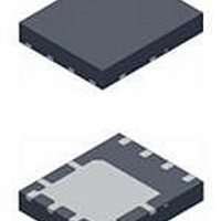
FDMS3602S Fairchild Semiconductor, FDMS3602S Datasheet - Page 12

FDMS3602S
Manufacturer Part Number
FDMS3602S
Description
MOSFET Power 25V Dual N-Channel PowerTrench MOSFET
Manufacturer
Fairchild Semiconductor
Datasheet
1.FDMS3602S.pdf
(15 pages)
Specifications of FDMS3602S
Configuration
Dual (MOSFET & SyncFET)
Transistor Polarity
Dual N-Channel
Resistance Drain-source Rds (on)
5.6 mOhms
Forward Transconductance Gfs (max / Min)
67 S
Drain-source Breakdown Voltage
25 V
Continuous Drain Current
15 A
Power Dissipation
2.2 W
Maximum Operating Temperature
+ 150 C
Mounting Style
SMD/SMT
Package / Case
Power 56
Module Configuration
Dual
Continuous Drain Current Id
40A
Drain Source Voltage Vds
25V
On Resistance Rds(on)
0.0044ohm
Rds(on) Test Voltage Vgs
10V
Lead Free Status / Rohs Status
Details
Figure 30. Shows the Power Stage in a buck converter topology
2. Recommended PCB Layout Guidelines
As a PCB designer, it is necessary to address critical issues in layout to minimize losses and optimize the performance of the power
train. Power Stage is a high power density solution and all high current flow paths, such as VIN (D1), PHASE (S1/D2) and GND (S2),
should be short and wide for better and stable current flow, heat radiation and system performance. A recommended layout proce-
dure is discussed below to maximize the electrical and thermal performance of the part.
Figure 31. Recommended PCB Layout
©2011 Fairchild Semiconductor Corporation
12
www.fairchildsemi.com
FDMS3602S Rev.C5


