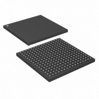
DS26528G+ Maxim Integrated Products, DS26528G+ Datasheet - Page 198

DS26528G+
Manufacturer Part Number
DS26528G+
Description
IC TXRX T1/E1/J1 OCT 256-CSBGA
Manufacturer
Maxim Integrated Products
Type
Transceiverr
Datasheet
1.DS26528G.pdf
(276 pages)
Specifications of DS26528G+
Number Of Drivers/receivers
4/4
Protocol
IEEE 1149.1
Voltage - Supply
3.135 V ~ 3.465 V
Mounting Type
Surface Mount
Package / Case
256-CSBGA
Lead Free Status / RoHS Status
Lead free / RoHS Compliant
- Current page: 198 of 276
- Download datasheet (2Mb)
Register Name:
Register Description:
Register Address:
Bit #
Name
Default
Note: See
Bit 7: TFDL Register Select (TFDLS).
Bit 6: Transmit SLC-96 (TSLC96). Set this bit to a one in SLC-96 framing applications. Must be set to source the
SLC-96 alignment pattern and data from the
Bit 4: F-Bit Corruption Type 2 (FBCT2). Setting this bit high enables the corruption of one Ft (D4 framing mode)
or FPS (ESF framing mode) bit in every 128 Ft or FPS bits as long as the bit remains set.
Bit 3: F-Bit Corruption Type 1 (FBCT1). A low-to-high transition of this bit causes the next three consecutive Ft
(D4 framing mode) or FPS (ESF framing mode) bits to be corrupted causing the remote end to experience a loss of
synchronization.
Bit 2: Transmit D4 RAI Select (TD4RM).
Bit 1: Pulse Density Enforcer Enable (PDE). The framer always examines both the transmit and receive data
streams for violations of the following rules which are required by ANSI T1.403: no more than 15 consecutive zeros
and at least N ones in each and every time window of 8 x (N +1) bits where N = 1 through 23. Violations for the
transmit and receive data streams are reported in the TLS1.3 and RLS2.7 bits, respectively. When this bit is set to
one, the DS26528 will force the transmitted stream to meet this requirement no matter the content of the
transmitted stream. When running B8ZS, this bit should be set to zero since B8ZS-encoded data streams cannot
violate the pulse density requirements.
Bit 0: Transmit-Side Bit 7 Zero-Suppression Enable (TB7ZS).
0 = source FDL or Fs bits from the internal TFDL register or the SLC-96 data formatter (TCR2.6)
1 = source FDL or Fs bits from the internal HDLC controller
0 = SLC-96 insertion disabled
1 = SLC-96 insertion enabled
0 = zeros in bit 2 of all channels
1 = a one in the S-bit position of frame 12
0 = disable transmit pulse density enforcer
1 = enable transmit pulse density enforcer
0 = no stuffing occurs
1 = force bit 7 to a one as determined by the GB7S bit at TCR1.3
TCR2
TFDLS
for E1 mode.
7
0
TSLC96
TCR2 (T1 Mode)
Transmit Control Register 2
182h + (200h x n): where n = 0 to 7, for Ports 1 to 8
6
0
—
5
0
T1TSLC1:T1TSLC3
198 of 276
FBCT2
4
0
registers. See Section
FBCT1
3
0
DS26528 Octal T1/E1/J1 Transceiver
TD4RM
2
0
8.9.4.4
PDE
1
0
for details.
TB7ZS
0
0
Related parts for DS26528G+
Image
Part Number
Description
Manufacturer
Datasheet
Request
R

Part Number:
Description:
MAX7528KCWPMaxim Integrated Products [CMOS Dual 8-Bit Buffered Multiplying DACs]
Manufacturer:
Maxim Integrated Products
Datasheet:

Part Number:
Description:
Single +5V, fully integrated, 1.25Gbps laser diode driver.
Manufacturer:
Maxim Integrated Products
Datasheet:

Part Number:
Description:
Single +5V, fully integrated, 155Mbps laser diode driver.
Manufacturer:
Maxim Integrated Products
Datasheet:

Part Number:
Description:
VRD11/VRD10, K8 Rev F 2/3/4-Phase PWM Controllers with Integrated Dual MOSFET Drivers
Manufacturer:
Maxim Integrated Products
Datasheet:

Part Number:
Description:
Highly Integrated Level 2 SMBus Battery Chargers
Manufacturer:
Maxim Integrated Products
Datasheet:

Part Number:
Description:
Current Monitor and Accumulator with Integrated Sense Resistor; ; Temperature Range: -40°C to +85°C
Manufacturer:
Maxim Integrated Products

Part Number:
Description:
TSSOP 14/A�/RS-485 Transceivers with Integrated 100O/120O Termination Resis
Manufacturer:
Maxim Integrated Products

Part Number:
Description:
TSSOP 14/A�/RS-485 Transceivers with Integrated 100O/120O Termination Resis
Manufacturer:
Maxim Integrated Products

Part Number:
Description:
QFN 16/A�/AC-DC and DC-DC Peak-Current-Mode Converters with Integrated Step
Manufacturer:
Maxim Integrated Products

Part Number:
Description:
TDFN/A/65V, 1A, 600KHZ, SYNCHRONOUS STEP-DOWN REGULATOR WITH INTEGRATED SWI
Manufacturer:
Maxim Integrated Products

Part Number:
Description:
Integrated Temperature Controller f
Manufacturer:
Maxim Integrated Products

Part Number:
Description:
SOT23-6/I�/45MHz to 650MHz, Integrated IF VCOs with Differential Output
Manufacturer:
Maxim Integrated Products

Part Number:
Description:
SOT23-6/I�/45MHz to 650MHz, Integrated IF VCOs with Differential Output
Manufacturer:
Maxim Integrated Products

Part Number:
Description:
EVALUATION KIT/2.4GHZ TO 2.5GHZ 802.11G/B RF TRANSCEIVER WITH INTEGRATED PA
Manufacturer:
Maxim Integrated Products

Part Number:
Description:
QFN/E/DUAL PCIE/SATA HIGH SPEED SWITCH WITH INTEGRATED BIAS RESISTOR
Manufacturer:
Maxim Integrated Products
Datasheet:


