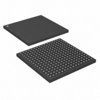
DS26528G+ Maxim Integrated Products, DS26528G+ Datasheet - Page 51

DS26528G+
Manufacturer Part Number
DS26528G+
Description
IC TXRX T1/E1/J1 OCT 256-CSBGA
Manufacturer
Maxim Integrated Products
Type
Transceiverr
Datasheet
1.DS26528G.pdf
(276 pages)
Specifications of DS26528G+
Number Of Drivers/receivers
4/4
Protocol
IEEE 1149.1
Voltage - Supply
3.135 V ~ 3.465 V
Mounting Type
Surface Mount
Package / Case
256-CSBGA
Lead Free Status / RoHS Status
Lead free / RoHS Compliant
- Current page: 51 of 276
- Download datasheet (2Mb)
8.9.4.1 Transmit-Signaling Operation
There are two methods to provide transmit-signaling data. These are processor based (i.e., software based) or
hardware based. Processor based refers to access through the transmit-signaling registers, TS1:TS16, while
hardware based refers to using the TSIG pins. Both methods can be used simultaneously.
8.9.4.1.1 Processor-Based Signaling
In processor-based mode, signaling data is loaded into the transmit-signaling registers (TS1:TS16) via the host
interface. On multiframe boundaries, the contents of these registers are loaded into a shift register for placement in
the appropriate bit position in the outgoing data stream. The user can use the transmit multiframe interrupt in
Latched Status Register 1 (TLS1.2) to know when to update the signaling bits. The user need not update any
transmit-signaling register for which there is no change of state for that register.
Each transmit-signaling register contains the robbed-bit signaling (TCR1.4 in T1 mode) or TS16 CAS signaling
(TCR1.6 in E1 mode) for one time slot that will be inserted into the outgoing stream. Signaling data can be sourced
from the TS registers on a per-channel basis by using the software-signaling insertion enable registers,
SSIE1:SSIE4.
In T1 ESF framing mode, there are four signaling bits per channel (A, B, C, and D). TS1:TS12 contain a full
multiframe of signaling data. In T1 D4 framing mode, there are only two signaling bits per channel (A and B). In T1
D4 framing mode, the framer uses A and B bit positions for the next multiframe. The C and D bit positions become
“don’t care” in D4 mode.
In E1 mode, TS16 carries the signaling information. This information can be in either CCS (common-channel
signaling) or CAS (channel-associated signaling) format. The 32 time slots are referenced by two different channel
number schemes in E1. In channel numbering, TS0 to TS31 are labeled channel 1 to channel 32. In phone channel
numbering, TS1 to TS15 are labeled channel 1 to channel 15, and TS17 to TS31 are labeled channel 15 to
channel 30.
8.9.4.2 Time Slot Numbering Schemes
TS
Channel
Phone
Channel
8.9.4.2.1 Hardware-Based Signaling
In hardware-based mode, signaling data is input via the TSIG pin. This signaling PCM stream is buffered and
inserted to the data stream being input at the TSER pin.
Signaling data can be input via the transmit hardware-signaling channel select (THSCS1) function. The framer can
be set up to take the signaling data presented at the TSIG pin and insert the signaling data into the PCM data
stream that is being input at the TSER pin. The user can control which channels are to have signaling data from the
TSIG pin inserted into them on a per-channel basis. The signaling insertion capabilities of the framer are available
whether the transmit-side elastic store is enabled or disabled. If the elastic store is enabled, the backplane clock
(TSYSCLK) can be either 1.544MHz or 2.048MHz.
0
1
1
2
1
2
3
2
3
4
3
4
5
4
5
6
5
6
7
6
7
8
7
8
9 10 11 12 13 14 15 16 17 18 19 20 21 22 23 24 25 26 27 28 29 30 31 32
8
9 10 11 12 13 14 15 16 17 18 19 20 21 22 23 24 25 26 27 28 29 30 31
9 10 11 12 13 14 15
51 of 276
16 17 18 19 20 21 22 23 24 25 26 27 28 29 30
DS26528 Octal T1/E1/J1 Transceiver
Related parts for DS26528G+
Image
Part Number
Description
Manufacturer
Datasheet
Request
R

Part Number:
Description:
MAX7528KCWPMaxim Integrated Products [CMOS Dual 8-Bit Buffered Multiplying DACs]
Manufacturer:
Maxim Integrated Products
Datasheet:

Part Number:
Description:
Single +5V, fully integrated, 1.25Gbps laser diode driver.
Manufacturer:
Maxim Integrated Products
Datasheet:

Part Number:
Description:
Single +5V, fully integrated, 155Mbps laser diode driver.
Manufacturer:
Maxim Integrated Products
Datasheet:

Part Number:
Description:
VRD11/VRD10, K8 Rev F 2/3/4-Phase PWM Controllers with Integrated Dual MOSFET Drivers
Manufacturer:
Maxim Integrated Products
Datasheet:

Part Number:
Description:
Highly Integrated Level 2 SMBus Battery Chargers
Manufacturer:
Maxim Integrated Products
Datasheet:

Part Number:
Description:
Current Monitor and Accumulator with Integrated Sense Resistor; ; Temperature Range: -40°C to +85°C
Manufacturer:
Maxim Integrated Products

Part Number:
Description:
TSSOP 14/A�/RS-485 Transceivers with Integrated 100O/120O Termination Resis
Manufacturer:
Maxim Integrated Products

Part Number:
Description:
TSSOP 14/A�/RS-485 Transceivers with Integrated 100O/120O Termination Resis
Manufacturer:
Maxim Integrated Products

Part Number:
Description:
QFN 16/A�/AC-DC and DC-DC Peak-Current-Mode Converters with Integrated Step
Manufacturer:
Maxim Integrated Products

Part Number:
Description:
TDFN/A/65V, 1A, 600KHZ, SYNCHRONOUS STEP-DOWN REGULATOR WITH INTEGRATED SWI
Manufacturer:
Maxim Integrated Products

Part Number:
Description:
Integrated Temperature Controller f
Manufacturer:
Maxim Integrated Products

Part Number:
Description:
SOT23-6/I�/45MHz to 650MHz, Integrated IF VCOs with Differential Output
Manufacturer:
Maxim Integrated Products

Part Number:
Description:
SOT23-6/I�/45MHz to 650MHz, Integrated IF VCOs with Differential Output
Manufacturer:
Maxim Integrated Products

Part Number:
Description:
EVALUATION KIT/2.4GHZ TO 2.5GHZ 802.11G/B RF TRANSCEIVER WITH INTEGRATED PA
Manufacturer:
Maxim Integrated Products

Part Number:
Description:
QFN/E/DUAL PCIE/SATA HIGH SPEED SWITCH WITH INTEGRATED BIAS RESISTOR
Manufacturer:
Maxim Integrated Products
Datasheet:


