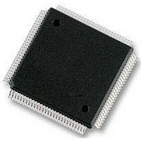
MC9S12E128CPV Freescale Semiconductor, MC9S12E128CPV Datasheet - Page 159

MC9S12E128CPV
Manufacturer Part Number
MC9S12E128CPV
Description
Microcontrollers (MCU) 16 Bit 16MHz
Manufacturer
Freescale Semiconductor
Datasheet
1.MC9S12E128CPV.pdf
(606 pages)
Specifications of MC9S12E128CPV
Data Bus Width
16 bit
Program Memory Type
Flash
Program Memory Size
128 KB
Data Ram Size
8 KB
Interface Type
SCI, SPI
Maximum Clock Frequency
25 MHz
Number Of Programmable I/os
92
Number Of Timers
16 bit
Operating Supply Voltage
3.135 V to 5.5 V
Maximum Operating Temperature
+ 85 C
Mounting Style
SMD/SMT
Package / Case
LQFP-112
Minimum Operating Temperature
- 40 C
On-chip Adc
10 bit
On-chip Dac
8 bit, 2 Channel
Lead Free Status / Rohs Status
No RoHS Version Available
Available stocks
Company
Part Number
Manufacturer
Quantity
Price
Company:
Part Number:
MC9S12E128CPVE
Manufacturer:
Freescale Semiconductor
Quantity:
10 000
- Current page: 159 of 606
- Download datasheet (4Mb)
3.4
Each pin associated with ports AD, M, P, Q, S, T and U can act as general-purpose I/O. In addition the pin
can act as an output from a peripheral module or an input to a peripheral module.
A set of configuration registers is common to all ports. All registers can be written at any time, however a
specific configuration might not become active.
3.4.1
The I/O Register holds the value driven out to the pin if the port is used as a general-purpose I/O. Writing
to the I/O Register only has an effect on the pin if the port is used as general-purpose output.
When reading the I/O Register, the value of each pin is returned if the corresponding Data Direction
Register bit is set to 0 (pin configured as input). If the data direction register bits is set to 1, the content of
the I/O Register bit is returned. This is independent of any other configuration
Due to internal synchronization circuits, it can take up to 2 bus cycles until the correct value is read on the
I/O Register when changing the data direction register.
3.4.2
The Input Register is a read-only register and generally returns the value of the pin
be used to detect overload or short circuit conditions.
Due to internal synchronization circuits, it can take up to 2 bus cycles until the correct value is read on the
Input Register when changing the Data Direction Register.
3.4.3
The Data Direction Register defines whether the pin is used as an input or an output. A Data Direction
Register bit set to 0 configures the pin as an input. A Data Direction Register bit set to 0 configures the pin
as an output. If a peripheral module controls the pin the contents of the data direction register is ignored
(Figure
Freescale Semiconductor
Example: Selecting a pull-up resistor. This resistor does not become active while the port is used
as a push-pull output.
3-49).
Functional Description
I/O Register
Input Register
Data Direction Register
MC9S12E128 Data Sheet, Rev. 1.07
Chapter 3 Port Integration Module (PIM9E128V1)
(Figure
(Figure
3-49).
3-49). It can
159
Related parts for MC9S12E128CPV
Image
Part Number
Description
Manufacturer
Datasheet
Request
R
Part Number:
Description:
Manufacturer:
Freescale Semiconductor, Inc
Datasheet:
Part Number:
Description:
Manufacturer:
Freescale Semiconductor, Inc
Datasheet:
Part Number:
Description:
Manufacturer:
Freescale Semiconductor, Inc
Datasheet:
Part Number:
Description:
Manufacturer:
Freescale Semiconductor, Inc
Datasheet:
Part Number:
Description:
Manufacturer:
Freescale Semiconductor, Inc
Datasheet:
Part Number:
Description:
Manufacturer:
Freescale Semiconductor, Inc
Datasheet:
Part Number:
Description:
Manufacturer:
Freescale Semiconductor, Inc
Datasheet:
Part Number:
Description:
Manufacturer:
Freescale Semiconductor, Inc
Datasheet:
Part Number:
Description:
Manufacturer:
Freescale Semiconductor, Inc
Datasheet:
Part Number:
Description:
Manufacturer:
Freescale Semiconductor, Inc
Datasheet:
Part Number:
Description:
Manufacturer:
Freescale Semiconductor, Inc
Datasheet:
Part Number:
Description:
Manufacturer:
Freescale Semiconductor, Inc
Datasheet:
Part Number:
Description:
Manufacturer:
Freescale Semiconductor, Inc
Datasheet:
Part Number:
Description:
Manufacturer:
Freescale Semiconductor, Inc
Datasheet:
Part Number:
Description:
Manufacturer:
Freescale Semiconductor, Inc
Datasheet:


