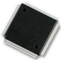
MC9S12E128CPV Freescale Semiconductor, MC9S12E128CPV Datasheet - Page 240

MC9S12E128CPV
Manufacturer Part Number
MC9S12E128CPV
Description
Microcontrollers (MCU) 16 Bit 16MHz
Manufacturer
Freescale Semiconductor
Datasheet
1.MC9S12E128CPV.pdf
(606 pages)
Specifications of MC9S12E128CPV
Data Bus Width
16 bit
Program Memory Type
Flash
Program Memory Size
128 KB
Data Ram Size
8 KB
Interface Type
SCI, SPI
Maximum Clock Frequency
25 MHz
Number Of Programmable I/os
92
Number Of Timers
16 bit
Operating Supply Voltage
3.135 V to 5.5 V
Maximum Operating Temperature
+ 85 C
Mounting Style
SMD/SMT
Package / Case
LQFP-112
Minimum Operating Temperature
- 40 C
On-chip Adc
10 bit
On-chip Dac
8 bit, 2 Channel
Lead Free Status / Rohs Status
No RoHS Version Available
Available stocks
Company
Part Number
Manufacturer
Quantity
Price
Company:
Part Number:
MC9S12E128CPVE
Manufacturer:
Freescale Semiconductor
Quantity:
10 000
- Current page: 240 of 606
- Download datasheet (4Mb)
Chapter 7 Digital-to-Analog Converter (DAC8B1CV1)
7.3.2
This section consists of register descriptions arranged in address order. Each description includes a
standard register diagram with an associated figure number. Details of register bit and field function follow
the register diagrams, in descending bit order.
7.3.2.1
Read: anytime (reserved locations read zero)
Write: anytime except DACTE is available only in special modes
240
Module Base + 0x0000
DACWAI
Reset
DACOE
DACTE
DSGN
DACE
Field
DJM
7
6
3
2
1
0
W
R
DACE
Register Descriptions
DAC Enable — This bit enables digital-to-analog converter functionality. When enabled, an analog voltage
based on the digital value in the DAC data register will be output. When disabled, DAO pin is high-impedance.
0 DAC is disabled and powered down
1 DAC is enabled for conversion
DAC Test Enable — This reserved bit is designed for factory test purposes only and is not intended for general
user access. Writing to this bit when in special test modes can alter DAC functionality.
Data Register Data Justification — This bit controls the justification of the data in the DAC data register
(DACD). If DJM is clear (left-justified), the data to be converted must be written to left justified DACD and the right
justified DACD register will read zeroes. If DJM is set (right-justified), the data to be converted is written to right
justified DACD register and left justified DACD register reads zeroes. Data is preserved if DJM bit is changed
after data is written.
0 Left justified data in DAC data register
1 Right justified data in DAC data register
Data Register Signed — This bit selects between signed and unsigned conversion data representation in the
DAC data register. Signed data is represented as 2’s complement.
0 Unsigned data representation in DAC data register
1 Signed data representation in DAC data register
DAC Stop in WAIT Mode — DACWAI disables the DAC8B1C module (no new conversion is done) during wait
mode.
0 DAC is enabled during wait mode
1 DAC is disabled and powered down during wait mode
DAC Output Enable — This bit enables the output on the DAO pin. To output the DAC voltage, the DACOE bit
and the DACE bit must be set. When disabled, DAO pin is high-impedance.
0 Output is not available for external use
1 Output on DAO pin enabled.
DAC Control Register 0 (DACC0)
0
7
= Unimplemented or Reserved
DACTE
0
6
Figure 7-3. DAC Control Register 0 (DACC0)
Table 7-2. DACC0 Field Descriptions
MC9S12E128 Data Sheet, Rev. 1.07
0
0
5
0
0
4
Description
DJM
0
3
DSGN
0
2
DACWAI
Freescale Semiconductor
0
1
DACOE
0
0
Related parts for MC9S12E128CPV
Image
Part Number
Description
Manufacturer
Datasheet
Request
R
Part Number:
Description:
Manufacturer:
Freescale Semiconductor, Inc
Datasheet:
Part Number:
Description:
Manufacturer:
Freescale Semiconductor, Inc
Datasheet:
Part Number:
Description:
Manufacturer:
Freescale Semiconductor, Inc
Datasheet:
Part Number:
Description:
Manufacturer:
Freescale Semiconductor, Inc
Datasheet:
Part Number:
Description:
Manufacturer:
Freescale Semiconductor, Inc
Datasheet:
Part Number:
Description:
Manufacturer:
Freescale Semiconductor, Inc
Datasheet:
Part Number:
Description:
Manufacturer:
Freescale Semiconductor, Inc
Datasheet:
Part Number:
Description:
Manufacturer:
Freescale Semiconductor, Inc
Datasheet:
Part Number:
Description:
Manufacturer:
Freescale Semiconductor, Inc
Datasheet:
Part Number:
Description:
Manufacturer:
Freescale Semiconductor, Inc
Datasheet:
Part Number:
Description:
Manufacturer:
Freescale Semiconductor, Inc
Datasheet:
Part Number:
Description:
Manufacturer:
Freescale Semiconductor, Inc
Datasheet:
Part Number:
Description:
Manufacturer:
Freescale Semiconductor, Inc
Datasheet:
Part Number:
Description:
Manufacturer:
Freescale Semiconductor, Inc
Datasheet:
Part Number:
Description:
Manufacturer:
Freescale Semiconductor, Inc
Datasheet:


