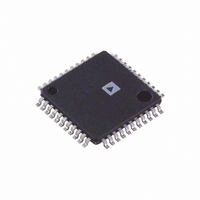
ADV7171KSU Analog Devices Inc, ADV7171KSU Datasheet - Page 34

ADV7171KSU
Manufacturer Part Number
ADV7171KSU
Description
IC DAC VIDEO ENC NTSC 44TQFP
Manufacturer
Analog Devices Inc
Type
Video Encoderr
Datasheet
1.ADV7171KSUZ.pdf
(64 pages)
Specifications of ADV7171KSU
Rohs Status
RoHS non-compliant
Applications
Set-Top Boxes, Video Players
Voltage - Supply, Analog
4.75 V ~ 5.25 V
Mounting Type
Surface Mount
Package / Case
44-TQFP, 44-VQFP
Adc/dac Resolution
10b
Screening Level
Industrial
Package Type
TQFP
Pin Count
44
Voltage - Supply, Digital
-
Lead Free Status / RoHS Status
Not Compliant
Available stocks
Company
Part Number
Manufacturer
Quantity
Price
Company:
Part Number:
ADV7171KSU
Manufacturer:
AD
Quantity:
319
Part Number:
ADV7171KSU
Manufacturer:
ADI/亚德诺
Quantity:
20 000
Company:
Part Number:
ADV7171KSUZ
Manufacturer:
LTC
Quantity:
20
Company:
Part Number:
ADV7171KSUZ
Manufacturer:
ADI
Quantity:
246
Company:
Part Number:
ADV7171KSUZ
Manufacturer:
Analog Devices Inc
Quantity:
10 000
Part Number:
ADV7171KSUZ
Manufacturer:
ADI/亚德诺
Quantity:
20 000
Company:
Part Number:
ADV7171KSUZ-REEL
Manufacturer:
SOURIAU
Quantity:
1 000
Company:
Part Number:
ADV7171KSUZ-REEL
Manufacturer:
Analog Devices Inc
Quantity:
10 000
ADV7170/ADV7171
TR0 BIT DESCRIPTION
Master/Slave Control (TR00)
This bit controls whether the ADV7170/ADV7171 is in
Master or Slave Mode.
Timing Mode Selection (TR02 to TR01)
These bits control the timing mode of the ADV7170/ ADV7171.
These modes are described in more detail in
the Timing and Control section.
BLANK Control (TR03)
This bit controls whether the BLANK input is used when the
part is in slave mode.
Luma Delay (TR05 to TR04)
These bits control the addition of a luminance delay. Each bit
represents a delay of 74 ns.
Pixel Port Control (TR06)
This bit is used to set the pixel port to accept 8-bit or 16-bit
data. If an 8-bit input is selected, the data will be set up on
Pin P7 to Pin P0.
Timing Register Reset (TR07)
Toggling TR07 from low to high and low again resets the
internal timing counters. This bit should be toggled after
power-up, reset or changing to a new timing mode.
REGISTER RESET
TR07
TIMING
TR07
TR06
PIXEL PORT
CONTROL
0
1
TR06
8 BIT
16 BIT
TR05 TR04
TR05
0
0
1
1
LUMA DELAY
0
1
0
1
Figure 43. Timing Register 0
Rev. C | Page 34 of 64
TR04
0ns DELAY
74ns DELAY
148ns DELAY
222ns DELAY
TR03
BLANK INPUT
0
1
CONTROL
TR03
ENABLE
DISABLE
TIMING MODE REGISTER 1 (TR17 TO TR10)
(Address (SR4 to SR0) = 08H)
Timing Register 1 is an 8-bit-wide register.
Figure 44 shows the various operations under the control of
Timing Register 1. This register can be read from as well written
to. This register can be used to adjust the width and position of
the master mode timing signals.
TR1 BIT DESCRIPTION
HSYNC Width (TR11 to TR10)
These bits adjust the HSYNC pulse width.
HSYNC to FIELD/VSYNC Delay (TR13 to TR12)
These bits adjust the position of the HSYNC output relative to
the FIELD/VSYNC output.
HSYNC to FIELD Rising Edge Delay (TR15 to TR14)
When the ADV7170/ADV7171 are in Timing Mode 1, these
bits adjust the position of the HSYNC output relative to the
FIELD output rising edge.
VSYNC Width (TR15 to TR14)
When the ADV7170/ADV7171 are configured in Timing
Mode 2, these bits adjust the VSYNC pulse width.
HSYNC to Pixel Data Adjust (TR17 to TR16)
This enables the HSYNC to be adjusted with respect to the pixel
data. This allows the Cr and Cb components to be swapped.
This adjustment is available in both master timing mode and
slave timing mode.
TR02 TR01
0
0
1
1
TIMING MODE
TR02
SELECTION
0
1
0
1
MODE 0
MODE 1
MODE 2
MODE 3
TR01
TR00
0
1
MASTER/SLAVE
CONTROL
SLAVE TIMING
MASTER TIMING
TR00


