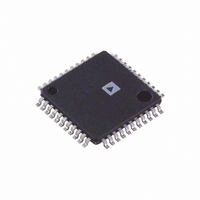
ADV7171KSU Analog Devices Inc, ADV7171KSU Datasheet - Page 37

ADV7171KSU
Manufacturer Part Number
ADV7171KSU
Description
IC DAC VIDEO ENC NTSC 44TQFP
Manufacturer
Analog Devices Inc
Type
Video Encoderr
Datasheet
1.ADV7171KSUZ.pdf
(64 pages)
Specifications of ADV7171KSU
Rohs Status
RoHS non-compliant
Applications
Set-Top Boxes, Video Players
Voltage - Supply, Analog
4.75 V ~ 5.25 V
Mounting Type
Surface Mount
Package / Case
44-TQFP, 44-VQFP
Adc/dac Resolution
10b
Screening Level
Industrial
Package Type
TQFP
Pin Count
44
Voltage - Supply, Digital
-
Lead Free Status / RoHS Status
Not Compliant
Available stocks
Company
Part Number
Manufacturer
Quantity
Price
Company:
Part Number:
ADV7171KSU
Manufacturer:
AD
Quantity:
319
Part Number:
ADV7171KSU
Manufacturer:
ADI/亚德诺
Quantity:
20 000
Company:
Part Number:
ADV7171KSUZ
Manufacturer:
LTC
Quantity:
20
Company:
Part Number:
ADV7171KSUZ
Manufacturer:
ADI
Quantity:
246
Company:
Part Number:
ADV7171KSUZ
Manufacturer:
Analog Devices Inc
Quantity:
10 000
Part Number:
ADV7171KSUZ
Manufacturer:
ADI/亚德诺
Quantity:
20 000
Company:
Part Number:
ADV7171KSUZ-REEL
Manufacturer:
SOURIAU
Quantity:
1 000
Company:
Part Number:
ADV7171KSUZ-REEL
Manufacturer:
Analog Devices Inc
Quantity:
10 000
CGMS_WSS REGISTER 1 C/W1 (C/W17 TO C/W10)
(Address [SR4 to SR0] = 17H)
CGMS_WSS Register 1 is an 8-bit-wide register. Figure 52
shows the operations under the control of this register.
C/W1 BIT DESCRIPTION
CGMS/WSS Data Bits (C/W15 to C/W10)
These bit locations are shared by CGMS data and WSS data. In
NTSC mode, these bits are CGMS data. In PAL mode, these bits
are WSS data.
CGMS DATA BITS (C/W17 TO C/W16)
These bits are CGMS data bits only.
C/W07
SIGNAL CONTROL
0
1
WIDE SCREEN
C/W17
C/W27
CGMS DATA BITS
C/W07
C/W17 – C/W16
TC07
DISABLE
ENABLE
TC07 TC06 TC05 TC04
0
0
"
1
1
TTXREQ RISING EDGE CONTROL
C/W06
CGMS EVEN FIELD
0
1
C/W16
C/W26
CONTROL
0
0
1
1
"
C/W06
TC06
DISABLE
ENABLE
0
0
1
1
"
C/W05
CGMS ODD FIELD
0
1
C/W25
CONTROL
C/W15
0
1
0
1
"
TC05
C/W05
DISABLE
ENABLE
Figure 50. Teletext Control Register
Figure 53. CGMS_ WSS Register 2
Figure 51. CGMS_WSS Register 0
Figure 52. CGMS_WSS Register 1
0 PCLK
1 PCLK
" PCLK
14 PCLK
15 PCLK
C/W04
CGMS CRC CHECK
0
1
Rev. C | Page 37 of 64
C/W24
CGMS/WSS DATA BITS
C/W14
CONTROL
TC04
C/W04
DISABLE
ENABLE
C/W27 – C/W20
C/W23
C/W13
TC03
CGMS/WSS DATA BITS
TC03 TC02 TC01 TC00
C/W03
CGMS_WSS REGISTER 2 C/W1 (C/W27 TO C/W20)
(Address [SR4 to SR0] = 18H)
CGMS_WSS Register 2 is an 8-bit-wide register. Figure 53
shows the operations under the control of this register.
C/W2 BIT DESCRIPTION
CGMS/WSS Data Bits (C/W27 to C/W20)
These bit locations are shared by CGMS data and WSS data. In
NTSC mode, these bits are CGMS data. In PAL mode, these bits
are WSS data.
0
0
"
1
1
TTXREQ FALLING EDGE CONTROL
C/W15 – C/W10
0
0
1
1
"
C/W22
C/W12
TC02
C/W02
CGMS DATA BITS
0
0
1
1
C/W03 – C/W00
"
0
1
0
1
"
C/W11
TC01
C/W21
C/W01
0 PCLK
1 PCLK
" PCLK
14 PCLK
15 PCLK
TC00
C/W20
C/W10
C/W00
ADV7170/ADV7171


