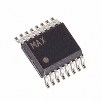
MXB7846EEE+T Maxim Integrated Products, MXB7846EEE+T Datasheet - Page 2

MXB7846EEE+T
Manufacturer Part Number
MXB7846EEE+T
Description
IC CNTRLR TOUCH RES 16QSOP
Manufacturer
Maxim Integrated Products
Type
Temperature Sensorr
Datasheet
1.MXB7846EEET.pdf
(24 pages)
Specifications of MXB7846EEE+T
Input Type
Analog
Output Type
Digital
Interface
4-Wire
Current - Supply
950µA
Mounting Type
Surface Mount
Package / Case
16-QSOP
Lead Free Status / RoHS Status
Lead free / RoHS Compliant
ABSOLUTE MAXIMUM RATINGS
V
Digital Outputs to GND...............................-0.3V to (V
V
Maximum Current into Any Pin .........................................±50mA
Maximum ESD per IEC-61000-4-2 (per MIL STD-883 HBM)
2.375V to 5.25V, 4-Wire Touch-Screen Controller
with Internal Reference and Temperature Sensor
ELECTRICAL CHARACTERISTICS
(V
T
Stresses beyond those listed under “Absolute Maximum Ratings” may cause permanent damage to the device. These are stress ratings only, and functional
operation of the device at these or any other conditions beyond those indicated in the operational sections of the specifications is not implied. Exposure to
absolute maximum rating conditions for extended periods may affect device reliability.
2
DD
REF
MIN
DC ACCURACY (Note 1)
Resolution
No Missing Codes
Relative Accuracy
Differential Nonlinearity
Offset Error
Gain Error
Noise
CONVERSION RATE
Conversion Time
Track/Hold Acquisition Time
Throughput Rate
Multiplexer Settling Time
Aperture Delay
Aperture Jitter
Channel-to-Channel Isolation
Serial Clock Frequency
Duty Cycle
ANALOG INPUT (X+, X-, Y+, Y-, AUX)
Input Voltage Range
Input Capacitance
Input Leakage Current
SWITCH DRIVERS
On-Resistance (Note 5)
INTERNAL REFERENCE
Reference Output Voltage
REF Output Tempco
REF Short-Circuit Current
REF Output Impedance
DD
X+, X-, Y+, Y-, VBAT, AUX ......................................15kV (4kV)
All Other Pins ..........................................................2kV (500V)
, VBAT, DIN, CS, DCLK to GND ........................-0.3V to +6V
_______________________________________________________________________________________
, X+, X-, Y+, Y-, AUX to GND..............-0.3V to (V
to T
= 2.7V to 3.6V, V
MAX
PARAMETER
, unless otherwise noted. Typical values are at T
REF
= 2.5V, f
DCLK
SYM B O L
f
TCV
SAMPLE
t
f
CONV
V
DNL
t
DCLK
INL
ACQ
REF
= 2MHz (50% duty cycle), f
REF
(Note 2)
(Note 3)
Including internal reference
12 clock cycles (Note 4)
16 clock conversion
V
On/off leakage, V
Y+, X+
Y-, X-
V
3 clock cycles
IN
DD
DD
DD
= 2.5V
= 2.7V to 5.25V, T
+ 0.3V)
+ 0.3V)
P-P
A
= +25°C.)
at 50kHz
CONDITIONS
IN
Continuous Power Dissipation (T
Operating Temperature Range ...........................-40°C to +85°C
Junction Temperature ......................................................+150°C
Storage Temperature Range .............................-65°C to +150°C
Lead Temperature (soldering, 10s) .................................+300°C
= 0 to V
SAMPLE
16-Pin QSOP (derate 8.30mW/°C above +70°C).........667mW
16-Pin TSSOP (derate 5.70mW/°C above +70°C) .......456mW
A
= +25°C
DD
= 125kHz, 12-bit mode, 0.1µF capacitor at REF, T
MIN
2.45
1.5
0.1
11
40
0
A
= +70°C)
TYP
±0.1
2.50
500
100
100
250
12
±1
±1
70
30
25
50
18
7
9
MAX
V
2.55
125
2.0
12
±2
±6
±4
60
±1
REF
6
ppm°/C
UNITS
µV
MHz
LSB
LSB
LSB
LSB
kHz
Bits
Bits
mA
dB
pF
µA
µs
µs
ns
ns
p s
%
Ω
Ω
RMS
V
V
A
=


