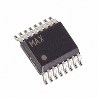
MXB7846EEE+T Maxim Integrated Products, MXB7846EEE+T Datasheet - Page 8

MXB7846EEE+T
Manufacturer Part Number
MXB7846EEE+T
Description
IC CNTRLR TOUCH RES 16QSOP
Manufacturer
Maxim Integrated Products
Type
Temperature Sensorr
Datasheet
1.MXB7846EEET.pdf
(24 pages)
Specifications of MXB7846EEE+T
Input Type
Analog
Output Type
Digital
Interface
4-Wire
Current - Supply
950µA
Mounting Type
Surface Mount
Package / Case
16-QSOP
Lead Free Status / RoHS Status
Lead free / RoHS Compliant
Figure 1. Detailed Serial Interface Timing
2.375V to 5.25V, 4-Wire Touch-Screen Controller
with Internal Reference and Temperature Sensor
8
_______________________________________________________________________________________
PIN
10
11
12
13
14
15
16
1
2
3
4
5
6
7
8
9
CS
DCLK
DIN
DOUT
BUSY
PENIRQ
NAME
DOUT
DCLK
BUSY
GND
AUX
V
BAT
REF
V
DIN
X+
Y+
CS
X-
Y-
DD
DD
Positive Supply Voltage. Connect to pin 10.
X+ Position Input, ADC Input Channel 1
Y+ Position Input, ADC Input Channel 2
X- Position Input
Y- Position Input
Ground
Battery Monitoring Inputs; ADC Input Channel 3
Auxiliary Input to ADC; ADC Input Channel 4
Voltage Reference Output/Input. Reference voltage for analog-to-digital conversion. In internal
reference mode, the reference buffer provides a 2.50V nominal output. In external reference mode,
apply a reference voltage between 1V and V
Positive Supply Voltage, +2.375V (2.70V) to +5.25V. External (internal) reference. Bypass with a 1µF
capacitor. Connect to pin 1.
Pen Interrupt Output. Open anode output. 10kΩ to 100kΩ pullup resistor required to V
Serial Data Output. Data changes state on the falling edge of DCLK. High impedance when CS is
HIGH.
Busy Output. BUSY pulses high for one clock period before the MSB decision. High impedance when
CS is HIGH.
Serial Data Input. Data clocked in on the rising edge of DCLK.
Active-Low Chip Select. Data is only clocked into DIN when CS is low. When CS is HIGH, DOUT and
BUSY are high impedance.
Serial Clock Input. Clocks data in and out of the serial interface and sets the conversion speed (duty
cycle must be 40% to 60%).
t
t
CSS
DV
t
DS
t
BDV
t
DH
t
CL
t
CH
t
CP
DD
t
BD
FUNCTION
. Bypass REF to GND with a 0.1µF capacitor.
t
DO
t
t
BTR
TR
Pin Description
t
CSH
DD
.


