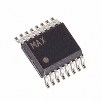
MXB7846EEE+T Maxim Integrated Products, MXB7846EEE+T Datasheet - Page 9

MXB7846EEE+T
Manufacturer Part Number
MXB7846EEE+T
Description
IC CNTRLR TOUCH RES 16QSOP
Manufacturer
Maxim Integrated Products
Type
Temperature Sensorr
Datasheet
1.MXB7846EEET.pdf
(24 pages)
Specifications of MXB7846EEE+T
Input Type
Analog
Output Type
Digital
Interface
4-Wire
Current - Supply
950µA
Mounting Type
Surface Mount
Package / Case
16-QSOP
Lead Free Status / RoHS Status
Lead free / RoHS Compliant
The MXB7846 uses a successive-approximation conver-
sion technique to convert analog signals to a 12-bit digi-
tal output. An SPI/QSPI/MICROWIRE™-compatible serial
interface provides easy communication to a micro-
processor (µP). It features an internal 2.5V reference, an
on-chip temperature sensor, a battery monitor, and a
4-wire touch-screen interface ( Functional Diagram ).
Figure 2 shows a block diagram of the analog input sec-
tion that includes the input multiplexer of the MXB7846,
the differential signal inputs of the ADC, and the differ-
ential reference inputs of the ADC. The input multiplexer
switches between X+, X-, Y+, Y-, AUX, BAT, and the
internal temperature sensor.
In single-ended mode, conversions are performed using
REF as the reference. In differential mode, ratiometric
conversions are performed with REF+ connected to X+ or
Y+, and REF- connected to X- or Y-. Configure the refer-
ence and switching matrix according to Tables 1 and 2.
with Internal Reference and Temperature Sensor
Figure 2. Equivalent Input Circuit
MICROWIRE is a trademark of National Semiconductor Corp.
2.375V to 5.25V, 4-Wire Touch-Screen Controller
V
GND
AUX
BAT
X+
Y+
X-
Y-
_______________________________________________________________________________________
PENIRQ
Detailed Description
Analog Inputs
TEMP1
7.5kΩ
TEMP0
2.5kΩ
BATTERY
ON
+V
During the acquisition interval, the selected channel
charges the sampling capacitance. The acquisition
interval starts on the fifth falling clock edge and ends
on the eighth falling clock edge.
The time required for the T/H to acquire an input signal
is a function of how quickly its input capacitance is
charged. If the input signal’s source impedance is high,
the acquisition time lengthens, and more time must be
allowed between conversions. The acquisition time
(t
the input signal to 12-bit accuracy. Calculate t
the following equation:
where R
the input signal.
Source impedances below 1kΩ do not significantly affect
the ADC’s performance. Accommodate higher source
impedances by either slowing down DCLK or by placing
a 1µF capacitor between the analog input and GND.
DD
ACQ
) is the maximum time the device takes to acquire
V
REF
IN
(SHOWN 001
t
ACQ
A2–A0
= 2kΩ and R
REFERENCE
B
)
2.5V
=
MXB7846
8 4
.
(SHOWN HIGH)
×
SER/DFR
S
(
R
is the source impedance of
S
REF ON/OFF
+IN
-IN
+
12-BIT ADC
R
REF+
REF-
IN
)
×
25
pF
ACQ
with
9


