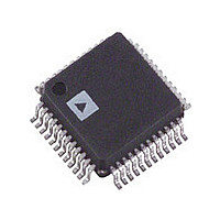
AD9849AKST Analog Devices Inc, AD9849AKST Datasheet - Page 11

AD9849AKST
Manufacturer Part Number
AD9849AKST
Description
IC CCD SIGNAL PROC 12BIT 48-LQFP
Manufacturer
Analog Devices Inc
Type
CCD Signal Processor, 12-Bitr
Datasheet
1.AD9849AKSTZRL.pdf
(32 pages)
Specifications of AD9849AKST
Rohs Status
RoHS non-compliant
Input Type
Logic
Output Type
Logic
Interface
3-Wire Serial
Mounting Type
Surface Mount
Package / Case
48-LQFP
Analog Front End Type
CCD
Analog Front End Category
Video
Interface Type
Serial (3-Wire)
Sample Rate
30MSPS
Input Voltage Range
0.5V
Operating Supply Voltage (min)
2.7/3V
Operating Supply Voltage (typ)
3/3.3/5V
Operating Supply Voltage (max)
3.6/5.5V
Resolution
12b
Number Of Adc's
1
Power Supply Type
Analog/Digital
Operating Temp Range
-20C to 85C
Operating Temperature Classification
Commercial
Mounting
Surface Mount
Pin Count
48
Package Type
LQFP
Number Of Channels
1
Current - Supply
-
Lead Free Status / RoHS Status
Not Compliant
Available stocks
Company
Part Number
Manufacturer
Quantity
Price
Company:
Part Number:
AD9849AKST
Manufacturer:
ADI
Quantity:
252
Part Number:
AD9849AKST
Manufacturer:
ADI/亚德诺
Quantity:
20 000
Company:
Part Number:
AD9849AKSTZ
Manufacturer:
Analog Devices Inc
Quantity:
10 000
Company:
Part Number:
AD9849AKSTZRL
Manufacturer:
Analog Devices Inc
Quantity:
10 000
SYSTEM OVERVIEW
Figures 1a and 1b show the typical system application diagrams
for the AD9848/AD9849. The CCD output is processed by the
AD9848/AD9849’s AFE circuitry, which consists of a CDS,
PxGA, VGA, black level clamp, and A/D converter. The
digitized pixel information is sent to the digital image
processor chip, where all post-processing and compression
occurs. To operate the CCD, CCD timing parameters are
programmed into the AD9848/AD9849 from the image
processor, through the 3-wire serial interface. From the system
master clock, CLI, provided by the image processor, the
AD9848/AD9849 generates the high speed CCD clocks and all
internal AFE clocks. All AD9848/AD9849 clocks are
synchronized with VD and HD.
Figure 1a shows the AD9848/AD9849 used in Internal Mode, in
which all the horizontal pulses (CLPOB, CLPDM, PBLK,
and HBLK) are programmed and generated internally. Figure 1b
shows the AD9848/AD9849 operating in External Mode, in
which the horizontal pulses are supplied externally by the
image processor.
The H-drivers for H1–H4 and RG are included in the AD9848/
AD9849, allowing these clocks to be directly connected to the
CCD. H-drive voltage of 5 V is supported in the AD9849.
REV. A
CCD
Figure 1a. Typical Application (Internal Mode)
H1–H4, RG
V-DRIVER
CCDIN
INTERFACE
SERIAL
AD9848/AD9849
INTEGRATED
AFE+TD
V1–V4, VSG1–VSG8, SUBCK
DOUT
HD, VD
CLI
DIGITAL IMAGE
PROCESSING
ASIC
–11–
Figure 2 shows the horizontal and vertical counter dimensions
for the AD9848/AD9849. All internal horizontal clocking is
programmed using these dimensions to specify line and
pixel locations.
CCD
Figure 1b. Typical Application (External Mode)
Figure 2. Vertical and Horizontal Counters
V-DRIVER
H1–H4, RG
CCDIN
12-BIT HORIZONTAL = 4096 PIXELS MAX
12-BIT VERTICAL = 4096 LINES MAX
MAXIMUM FIELD DIMENSIONS
INTERFACE
SERIAL
AD9848/AD9849
INTEGRATED
AFE+TD
AD9848/AD9849
V1–V4, VSG1–VSG8, SUBCK
CLPDM
CLPOB
HD, VD
DOUT
HBLK
PBLK
CLI
DIGITAL IMAGE
PROCESSING
ASIC


