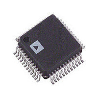
AD9849AKST Analog Devices Inc, AD9849AKST Datasheet - Page 29

AD9849AKST
Manufacturer Part Number
AD9849AKST
Description
IC CCD SIGNAL PROC 12BIT 48-LQFP
Manufacturer
Analog Devices Inc
Type
CCD Signal Processor, 12-Bitr
Datasheet
1.AD9849AKSTZRL.pdf
(32 pages)
Specifications of AD9849AKST
Rohs Status
RoHS non-compliant
Input Type
Logic
Output Type
Logic
Interface
3-Wire Serial
Mounting Type
Surface Mount
Package / Case
48-LQFP
Analog Front End Type
CCD
Analog Front End Category
Video
Interface Type
Serial (3-Wire)
Sample Rate
30MSPS
Input Voltage Range
0.5V
Operating Supply Voltage (min)
2.7/3V
Operating Supply Voltage (typ)
3/3.3/5V
Operating Supply Voltage (max)
3.6/5.5V
Resolution
12b
Number Of Adc's
1
Power Supply Type
Analog/Digital
Operating Temp Range
-20C to 85C
Operating Temperature Classification
Commercial
Mounting
Surface Mount
Pin Count
48
Package Type
LQFP
Number Of Channels
1
Current - Supply
-
Lead Free Status / RoHS Status
Not Compliant
Available stocks
Company
Part Number
Manufacturer
Quantity
Price
Company:
Part Number:
AD9849AKST
Manufacturer:
ADI
Quantity:
252
Part Number:
AD9849AKST
Manufacturer:
ADI/亚德诺
Quantity:
20 000
Company:
Part Number:
AD9849AKSTZ
Manufacturer:
Analog Devices Inc
Quantity:
10 000
Company:
Part Number:
AD9849AKSTZRL
Manufacturer:
Analog Devices Inc
Quantity:
10 000
Driving the CLI Input
The AD9848/AD9849’s master clock input (CLI) may be used in
two different configurations, depending on the application.
Figure 23a shows a typical dc-coupled input from the master clock
source. When the dc-coupled technique is used, the master clock
signal should be at standard 3 V CMOS logic levels. As shown in
Figure 23b, a 1000 pF ac-coupling capacitor may be used between
the clock source and the CLI input. In this configuration, the
CLI input will self-bias to the proper dc voltage level of approxi-
mately 1.4 V. When the ac-coupled technique is used, the
master clock signal can be as low as ± 500 mV in amplitude.
REV. A
SUPPLY
DRIVER
3V
OUTPUTS
DATA
0.1 F
12
Figure 21. Recommend Circuit Configuration for External Mode
H DRIVER
SUPPLY
RG DRIVER
SUPPLY
(MSB) D11
DVDD3
DVSS3
DIGITAL
SUPPLY
D10
D2
D3
D4
D5
D6
D7
D8
D9
3V
10
11
12
1
2
3
4
5
6
8
9
7
0.1 F
48 47 46 45 44
13 14 15 16
PIN 1
IDENTIFIER
0.1 F
(Not to Scale)
17 18 19 20 21 22 23 24
TOP VIEW
AD9849
43 42 41 40
0.1 F
–29–
39 38 37
H3
0.1 F
17
36
35
34
33
32
31
30
29
28
27
26
25
SL
REFT
REFB
CMLEVEL
AVSS3
AVDD3
BYP3
CCDIN
BYP2
BYP1
AVDD2
AVSS2
Figure 22a. CCD Connections (2 H-Clock)
H4
18
5
AD9848/AD9849
3V
ANALOG
SUPPLY
H1
HIGH SPEED
CLOCKS
13
H1
0.1 F 0.1 F 0.1 F
H2
CLOCK
INPUT
14
H2
0.1 F
1 F
1 F
6
3
CCD IMAGER
INTERFACE
RG
CLOCK
INPUTS
SERIAL
20
RG
AD9848/AD9849
SIGNAL
0.1 F
0.1 F
OUT
0.1 F
29
CCDIN
3V
ANALOG
SUPPLY
3V
ANALOG
SUPPLY
CCD
SIGNAL


