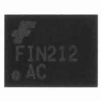
FIN212ACGFX Fairchild Semiconductor, FIN212ACGFX Datasheet - Page 9

FIN212ACGFX
Manufacturer Part Number
FIN212ACGFX
Description
IC SER/DESER 12BIT 42USS-BGA
Manufacturer
Fairchild Semiconductor
Series
SerDes™r
Datasheet
1.FIN212ACGFX.pdf
(16 pages)
Specifications of FIN212ACGFX
Function
Serializer/Deserializer
Data Rate
560Mbps
Input Type
LVCMOS
Output Type
LVCMOS
Number Of Inputs
12
Number Of Outputs
12
Voltage - Supply
1.65 V ~ 3.6 V
Operating Temperature
-30°C ~ 70°C
Mounting Type
Surface Mount
Package / Case
42-BGA
Lead Free Status / RoHS Status
Lead free / RoHS Compliant
Other names
FIN212ACGFXTR
Available stocks
Company
Part Number
Manufacturer
Quantity
Price
Company:
Part Number:
FIN212ACGFX
Manufacturer:
FSC
Quantity:
4 964
Company:
Part Number:
FIN212ACGFX
Manufacturer:
Fairchild Semiconductor
Quantity:
10 000
DC Electrical Characteristics
Notes:
3.
4.
Power Supply Currents
Pin Capacitance Tables
Symbol
C
© 2008 Fairchild Semiconductor Corporation
FIN212AC • Rev. 1.1.0
DIFFERENTIAL I/O
Symbol
I
I
DD_SER1
DD_DES1
IN
I
DD_PD
R
, C
I
V
I
V
V
ODH
ODL
I
TRM
Typical values are given for V
and negative values refer to the current flowing out of pins. Voltages are referenced to GROUND unless otherwise
specified (except ΔV
V
OH
IN
GO
OL
IO
GO
, C
is the difference in device ground levels between the CTL driver and the CTL receiver.
IO-DIFF
Parameter
V
Dynamic Serializer Power Supply
Current
Dynamic Deserializer Power
Supply Current
Output High Voltage
Output Low Voltage
Input Current
Output HIGH
Source Current
Output LOW
Sink Current
Input Voltage Ground Offset
CKS Internal Receiver
Termination Resistor
DS Internal Receiver
Termination Resistor
DD
Power-Down Supply Current
Parameter
Capacitance of Input Only Signals; Parallel
Port Pins DP[1:10]; Differential I/O
OD
and V
V
V
OS
OS
OD
DD
=1.0V
=1.0V
).
=2.775V and T
(4)
(Continued)
DIRI=0
CTL_ADJ=0
CTL_ADJ=1
CTL_ADJ=0
CTL_ADJ=1
V
DIRI=0
V
I
I
I
I
I
I
V
OH
OH
OH
OL
OL
OL
ID
ID
IN
Test Conditions
S1=S0=0, All Inputs at GND or VDD
f
PLL1=0,PLL0=1;
CTL_ADJ=0; C
f
PLL1=0,PLL0=1;
CTL_ADJ=0; C
CKREF
CKREF
=2.0mA, S1=0,S0=1
=0.4mA, S1=1,S0=0
=1.0mA, S1=1,S0=1
=50mV, V
=50mV, V
=-2.0mA, S1=0,S0=1
=-0.4mA, S1=1,S0=0
=-1.0mA, S1=1,S0=1
= 0V to 3.6V
A
=f
=f
=25°C. Positive current values refer to the current flowing into the device
STRB
STRB,
IC
IC
,
=925mV,
=925mV,
L
L
=0pF
=0pF
Test Conditions
DIRI=1, S1=0, S0=0,
V
9
DD
=2.5V
S1=L
S0=H
S1=H
S0=L
S1=H
S0=H
S1=L
S0=H
S1=H
S0=L
S1=H
S0=H
0.75xV
-5.0
80
80
0
DDP
20MHz
40MHz
5MHz
14MHz
8MHz
28MHz
20MHz
40MHz
5MHz
14MHz
8MHz
28MHz
Min.
-3.4
100
100
1.2
-2
2
0
Min.
Typ.
2
Typ.
0.1
9.5
13
19
17
11
20
10
14
12
8
9
9
0.25xV
www.fairchildsemi.com
V
120
120
Max.
5.0
DDP
Max.
DDP
Unit
pF
Unit
mA
mA
mA
mA
mA
mA
mA
mA
mA
mA
mA
mA
mA
mA
µA
µA
Ω
Ω
V
V
V


