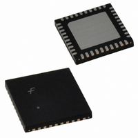
FIN24ACMLX Fairchild Semiconductor, FIN24ACMLX Datasheet - Page 11

FIN24ACMLX
Manufacturer Part Number
FIN24ACMLX
Description
IC SERIALIZER/DESERIALZR 40MLP
Manufacturer
Fairchild Semiconductor
Series
SerDes™r
Datasheet
1.FIN24ACMLX.pdf
(25 pages)
Specifications of FIN24ACMLX
Function
Serializer/Deserializer
Data Rate
520Mbps
Input Type
LVCMOS
Output Type
LVCMOS
Number Of Inputs
20
Number Of Outputs
20
Voltage - Supply
1.65 V ~ 3.6 V
Operating Temperature
-30°C ~ 70°C
Mounting Type
Surface Mount
Package / Case
40-MLP
Lead Free Status / RoHS Status
Lead free / RoHS Compliant
© 2005 Fairchild Semiconductor Corporation
FIN24AC Rev. 1.0.3
Application Mode Diagrams
Figure 11 shows basic operation when a pair of SerDes is configured in an unidirectional operation mode.
In Master Operation, the device:
1. Is configured as a serializer at power-up based on the
2. Accepts CKREF_M word clock and generates a bit
3. Receives parallel data on the rising edge of
4. Generates and transmits serialized data on the
5. Generates an embedded word clock for each strobe
value of the DIRI signal.
clock with embedded word boundary. This bit clock is
sent to the slave device through the CKSO port.
STROBE_M.
signal.
DS signals source synchronously with CKSO.
STROBE_M
DP[1:12]_M
CKREF_M
Note:
Data on serializer pins DP[21:22] is output on pins DP[23:24] of the deserializer.
Master Device Operating as a Serializer
Sending
Unit
Figure 11. Simplified Block Diagram for Unidirectional Serializer and Deserializer
REFCK
DATA [0:19]
CNTL[0:1]
S2 = S1 = “0”
DIR = “1”
V
DD
Figure 12. Unidirectional Serializer and Deserializer
PLL
Serializer
Control
CKREF
STROBE
DP[21:22]
DP[1:20]
S1
S2
DIRI
Serializer
Unidirectional Data Transfer
BIT CK
Gen.
FIN24AC
CKSO
CKSO
+
–
+
–
DS
DS
11
CKSI
In Slave Operation, the device:
1. Is configured as a deserializer at power-up based on
2. Accepts an embedded word boundary bit clock on
3. Deserializes the DS data stream using the CKSI input
4. Writes parallel data onto the DP_S port and generates
+
–
+
–
Slave Device Operating as a Deserializer
CKSI
DS
the value of the DIRI signal.
CKSI.
clock.
the CKP_S. CKP_S is only generated when a valid
data word occurs.
Deserializer
Deserializer
FIN24AC
Control
DP[23:24]
DP[1:20]
CKP
DIRI
S1
S2
Work CK
Gen
S2 = S1 = “0”
DIR = “0”
DATA [0:19]
CNTL[0:1]
Receiving
CKP_S
DP[1:12]_S
Unit
www.fairchildsemi.com


