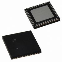
FIN24ACMLX Fairchild Semiconductor, FIN24ACMLX Datasheet - Page 14

FIN24ACMLX
Manufacturer Part Number
FIN24ACMLX
Description
IC SERIALIZER/DESERIALZR 40MLP
Manufacturer
Fairchild Semiconductor
Series
SerDes™r
Datasheet
1.FIN24ACMLX.pdf
(25 pages)
Specifications of FIN24ACMLX
Function
Serializer/Deserializer
Data Rate
520Mbps
Input Type
LVCMOS
Output Type
LVCMOS
Number Of Inputs
20
Number Of Outputs
20
Voltage - Supply
1.65 V ~ 3.6 V
Operating Temperature
-30°C ~ 70°C
Mounting Type
Surface Mount
Package / Case
40-MLP
Lead Free Status / RoHS Status
Lead free / RoHS Compliant
© 2005 Fairchild Semiconductor Corporation
FIN24AC Rev. 1.0.3
DC Electrical Characteristics
Values are provided for over-supply voltage and operating temperature ranges, unless otherwise specified.
Notes:
2. Typical Values are given for V
3. V
LVCMOS I/O
DIFFERENTIAL I/O
Symbol
R
R
and negative values means current flowing out of pins. Voltage is referenced to GROUND unless otherwise specified
(except ΔV
I
V
I
V
V
V
V
ODH
ODL
I
V
I
I
TRM
TRM
GO
OZ
ICM
GO
OH
OL
IN
IZ
IH
IL
is the difference in device ground levels between the CTL driver and the CTL receiver.
Input High Voltage
Input Low Voltage
Output High Voltage
Output Low Voltage
Input Current
Output High Source
Current
Output Low Sink Current
Disabled Output Leakage
Current
Disabled Input Leakage
Current
Input Common Mode Range V
Input Voltage Ground
Off-set Relative to Driver
CKSI Internal Receiver
Termination Resistor
DSI Internal Receiver,
Termination Resistor
OD
and V
Parameter
OD
).
DD
= 2.775V and T
(3)
I
I
V
V
V
CKSO, DSO = 0V to V
S2 = S1 = 0V
CKSI, DSI = 0V to V
S2 = S1 = 0V
See Figure 15
V
0, | CKSI+ – CKSI- | = V
V
0, | DSI+ – DSI- | = V
OH
OL
IN
OS
OS
DDS
ID
ID
= 2.0 mA
= –2.0 mA
= 0V to 3.6V
= 50mV, V
= 50mV, V
= 1.0V, Figure 14
= 1.0V, Figure 14
= 2.775 ± 5%
Test Conditions
A
= 25°C. Positive current values refer to the current flowing into device
IC
IC
V
V
V
V
V
V
= 925mV, DIRI =
= 925mV, DIRI =
DDP
DDP
DDP
DDP
DDP
DDP
14
DDS
ID
= 3.3 ± 0.3
= 2.5 ± 0.2
= 1.8 ± 0.15
= 3.3 ± 0.3
= 2.5 ± 0.2
= 1.8 ± 0.15
DDS
,
ID
,
0.65 x V
0.75 x V
Min.
GND
–5.0
80.0
80.0
DDP
DDP
V
GO
Typ.
–1.75
0.950
±0.1
±0.1
100
100
+ 0.80
0
(2)
0.35 x V
0.25 x V
Max.
V
±5.0
±5.0
120
120
5.0
DDP
www.fairchildsemi.com
DDP
DDP
Unit
mA
mA
µA
µA
µA
Ω
Ω
V
V
V
V
V


