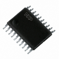
PCA9544APW,112 NXP Semiconductors, PCA9544APW,112 Datasheet - Page 16

PCA9544APW,112
Manufacturer Part Number
PCA9544APW,112
Description
IC I2C MUX 4CH BI-DIR 20-TSSOP
Manufacturer
NXP Semiconductors
Datasheet
1.PCA9544ABS118.pdf
(26 pages)
Specifications of PCA9544APW,112
Package / Case
20-TSSOP
Applications
4-Channel I²C Multiplexer
Interface
I²C
Voltage - Supply
2.3 V ~ 3.6 V, 4.5 V ~ 5.5 V
Mounting Type
Surface Mount
Product
Decoders, Encoders, Multiplexers & Demultiplexers
Logic Family
PCA
Number Of Lines (input / Output)
8.0 / 10.0
Propagation Delay Time
0.3 ns
Supply Voltage (max)
5.5 V
Supply Voltage (min)
2.3 V
Maximum Operating Temperature
+ 85 C
Minimum Operating Temperature
- 40 C
Mounting Style
SMD/SMT
Number Of Input Lines
8.0
Number Of Output Lines
10.0
Power Dissipation
400 mW
Lead Free Status / RoHS Status
Lead free / RoHS Compliant
Lead Free Status / RoHS Status
Lead free / RoHS Compliant, Lead free / RoHS Compliant
Other names
568-1045-5
935275806112
PCA9544APW
935275806112
PCA9544APW
NXP Semiconductors
11. Dynamic characteristics
Table 9.
[1]
[2]
[3]
[4]
[5]
PCA9544A_4
Product data sheet
Symbol
t
f
t
t
t
t
t
t
t
t
t
t
C
t
t
t
INT
t
t
t
t
PD
SCL
BUF
HD;STA
LOW
HIGH
SU;STA
SU;STO
HD;DAT
SU;DAT
r
f
SP
VD;DAT
VD;ACK
v(INTnN-INTN)
d(INTnN-INTN)
w(rej)L
w(rej)H
b
Pass gate propagation delay is calculated from the 20
After this period, the first clock pulse is generated.
A device must internally provide a hold time of at least 300 ns for the SDA signal (referred to the V
bridge the undefined region of the falling edge of SCL.
C
Measurements taken with 1 k pull-up resistor and 50 pF load.
b
= total capacitance of one bus line in pF.
Dynamic characteristics
Parameter
propagation delay
SCL clock frequency
bus free time between a STOP and
START condition
hold time (repeated) START
condition
LOW period of the SCL clock
HIGH period of the SCL clock
set-up time for a repeated START
condition
set-up time for STOP condition
data hold time
data set-up time
rise time of both SDA and SCL
signals
fall time of both SDA and SCL
signals
capacitive load for each bus line
pulse width of spikes that must be
suppressed by the input filter
data valid time
data valid acknowledge time
valid time from INTn to INT signal
delay time from INTn to INT inactive
LOW-level rejection time
HIGH-level rejection time
Rev. 04 — 15 June 2009
Conditions
from SDA to SDx,
or SCL to SCx
HIGH-to-LOW
LOW-to-HIGH
INTn inputs
INTn inputs
typical R
on
and the 15 pF load capacitance.
4-channel I
[2]
[5]
[5]
[5]
[5]
[5]
[5]
Standard-mode
Min
250
4.7
4.0
4.7
4.0
4.7
4.0
0
0.5
2
0
1
-
[3]
-
-
-
-
-
-
-
-
-
C-bus multiplexer with interrupt logic
I
2
C-bus
0.3
1000
Max
3.45
100
300
400
0.6
50
1
1
4
2
-
-
-
-
-
-
-
-
-
[1]
IH(min)
20 + 0.1C
20 + 0.1C
Fast-mode I
of the SCL signal) in order to
PCA9544A
Min
100
1.3
0.6
1.3
0.6
0.6
0.6
0
0.5
0
1
-
-
-
-
-
-
-
-
[3]
© NXP B.V. 2009. All rights reserved.
b
b
[4]
[4]
2
C-bus
0.3
Max
400
300
300
400
0.9
0.6
50
1
1
4
2
-
-
-
-
-
-
-
-
-
[1]
16 of 26
Unit
ns
kHz
ns
ns
ns
pF
ns
s
s
s
s
s
s
s
s
s
s
s
s
s
s


