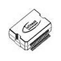
TLE6240GPNT Infineon Technologies, TLE6240GPNT Datasheet - Page 12

TLE6240GPNT
Manufacturer Part Number
TLE6240GPNT
Description
Manufacturer
Infineon Technologies
Datasheet
1.TLE6240GPNT.pdf
(37 pages)
Specifications of TLE6240GPNT
Switch Type
Low Side
Power Switch Family
TLE6240
Input Voltage
-0.3 to 7V
Power Switch On Resistance
1Ohm
Output Current
500mA
Number Of Outputs
16
Mounting
Surface Mount
Supply Current
5mA
Package Type
DSO
Operating Temperature (min)
-40C
Operating Temperature (max)
150C
Operating Temperature Classification
Automotive
Pin Count
36
Lead Free Status / Rohs Status
Compliant
5
The TLE6240GP is an 16-fold low-side power switch which provides a serial peripheral interface (SPI) to control
the 16 power DMOS switches, and diagnostic feedback. The power transistors are protected against short to
overload, overtemperature and against overvoltage by active zener clamp.
The diagnostic logic recognizes a fault condition which can be read out via the serial diagnostic output (SO).
5.1
RESET - Reset pin. If the reset pin is in a logic low state, it clears the SPI shift register and switches all outputs
OFF. An internal pull-up structure is provided on chip. In case the RESET Pin is pulled down statically, the device
remains in Stand-by Mode
Electrical Characteristics: Power Supply
V
all voltages with respect to ground, positive current flowing into pin
Pos.
5.1.1
5.1.2
5.1.3
1) For
5.2
In this chapter is the electrical behavior of the following Digital Input Pins described:
•
•
•
Electrical Characteristics: Digital Inputs
V
all voltages with respect to ground, positive current flowing into pin
Pos.
5.2.1
5.2.2
5.2.3
5.2.4
5.2.5
5.2.6
Data Sheet
S
S
= 4.5 V to 5.5 V,
= 4.5 V to 5.5 V,
undervoltage reset gets active at
parallel Input Pin INx
Reset Pin RESET
Program Pin PRG
V
S
Parameter
Supply Voltage
Supply Current
Supply Current in Standby Mode
Parameter
Input Low Voltage
Input High Voltage
Input Voltage Hysteresis
Input Pull-down/up Current
(IN1 to IN4, IN9 to IN12)
PRG, Reset Pull-up Current
Minimum Reset Duration
(After a reset all parallel inputs are
ORed with the SPI data bits)
< 4.5 V the power stages are switched according the input signals and data bits or are definitely switched off. This
Electrical and Functional Description of Blocks
Power Supply & Reset
Digital Inputs
T
T
j
j
= -40 °C to +150 °C, Reset = H (unless otherwise specified)
= -40 °C to +150 °C, Reset = H (unless otherwise specified)
1)
V
S
= 3 V (typ. value) and is specified by design and not subject to production test.
Symbol
V
I
I
Symbol
V
V
V
I
I
t
Reset,min
IN(1..4,9..12)
IN(PRG,Res)
S
S(stdy)
S
INL
INH
INHys
12
Min.
4.5
–
–
Min.
-0.3
2.0
50
20
20
10
Electrical and Functional Description of Blocks
Limit Values
Limit Values
Typ.
–
5
10
–
100
50
50
–
Typ.
–
Smart 16-Channel Low-Side Switch
Max.
5.5
10
50
Max.
1.0
–
200
100
100
–
Unit
V
mA
µA
Unit
V
V
mV
µA
µA
µs
Rev.3.3, 2010-02-15
Conditions
–
–
(RESET = L)
Conditions
–
–
–
V
–
–
IN
= 5 V
TLE6240GP
V
BB
,


